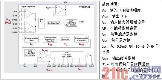
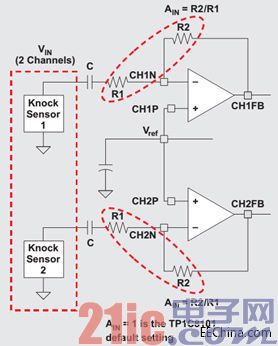
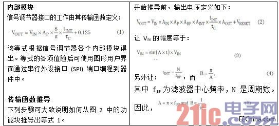
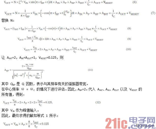
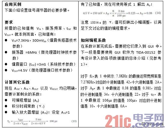
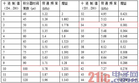
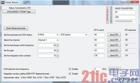
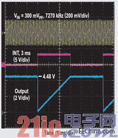
If the ignition time is incorrect or the component is faulty, the engine cylinder will knock. Modern vehicles have a knock sensor system on the engine that minimizes knock, maximizing engine life, increasing power and improving fuel efficiency. This article will discuss the basics of engine knocking and how to set up a knock sensor signal conditioning system. This article refers to the address: http:// Engine knock basics Engine knock is the uncontrolled ignition of a fuel-air mixture in a cylinder rather than being ignited by a spark plug. Engine knock can significantly increase cylinder pressure and damage engine components, causing a “clickâ€. In the normal combustion state, the internal combustion engine combusts the fuel-air mixture in a controlled manner. Combustion should initiate several crank angles before the piston passes through the apex directly above. This timing advance is necessary because it takes some time for the fuel-air mixture to completely burn, and this time varies with engine speed and load changes. If the timing is appropriate, the maximum cylinder pressure will produce several crank angles after the piston passes the apex directly above. The fully combusted fuel-air mixture then pushes the piston down with maximum force, creating the maximum torque applied to the crankshaft per cycle. The current engine has been carefully designed to minimize emissions and maximize power and fuel economy. This can be achieved by optimizing the ignition spark timing to maximize torque. Through this timing control, the spark plug can not only ignite the fuel-air mixture from the ignition point to the cylinder wall, but also can burn evenly at a certain rate. If you deviate from normal combustion, such as ignition too fast, it will cause engine knock. And in extreme cases it can cause permanent damage to the engine. Other conditions that cause engine knock include the use of incorrect octane gasoline or defective ignition components. Signal conditioner interface Modern cars have a knock sensor system that detects the knocking of each cylinder at a specific time after crossing the upper apex, called the knock window. The system typically consists of a piezoelectric sensing element and a signal conditioner. The sensor detects vibration and the signal processor processes the signal and sends a voltage signal to the engine control module. The module interprets the knock signal, which not only controls timing but also improves engine efficiency. The knock sensor is typically mounted on the engine block (Figure 1). Figure 1: Knock sensor mounted on the engine block Figure 2: Block diagram of the TPIC8101 with coefficients The simplified diagram shown in Figure 2 is a TPIC8101 dual-channel, highly integrated signal conditioner interface from Texas Instruments that can be used to connect knock sensor components to engine control modules. Two internal broadband amplifiers (Figure 3) provide an interface to the piezoelectric sensor. The output of the amplifier is provided to the channel selection multiplexer switch (Figure 2) and then to the third-order de-glitch filter (AAF). This signal is then converted using an analog-to-digital converter (ADC) before the programmable gain stage. The gain stage can feed the signal to a programmable bandpass filter for processing specific frequency components associated with the engine and knock sensor. After the full-wave rectification of the output of the bandpass filter, the integral operation can be completed according to the programmed time constant and the integration time period. The integrator output is reset when each knock window is activated. The integrated signal is converted to an analog format by a digital-to-analog converter (DAC), but can be directly connected to the microprocessor. The processor not only reads the data, but also adjusts the spark ignition timing to optimize fuel efficiency based on load and engine speed while reducing knock. Figure 3: Input Amplifier Interface Details The integrator works from 0 to B for N times. This will override the positive input. Full-wave rectification can then be compensated by other gain factors. Replace VIN, from 0 to 1/fBP integral. Table 1: Partial SPI Lookup Table on page 10 of the TPIC8101 Product Specification Figure 4: GUI values Figure 5: Example Waveform Enter 6MHz in the vibrator frequency and 1 in the number of channels. The GUI value should be similar to that shown in Figure 4. According to the above steps, the waveform shown in Fig. 5 can be obtained. For more waveforms with different amplitude modulations, refer to the TIDA-00152 Reference Design Test Data in Reference 1. in conclusion To achieve the desired engine performance and protect the engine, engine knock control must be performed. The dual input and advanced signal conditioning of the TPIC8101 knock sensor interface reduces the processing load on the engine control module. Usually,10 & 20 layers PCB are HDI board,but some are not .Some with big trace width and space,holes are over 0.3mm too. We have much experience in doing 10 Layer PCB & 20 layer PCB. 10 Layer PCB 10 layer PCB 10 layer TG170 PCB 10 layer design Storm Circuit Technology Ltd , https://www.stormpcb.com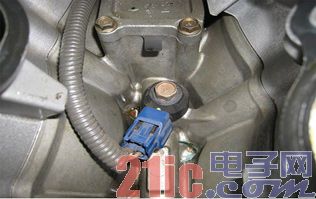
A ten-layer board should be used when six routing layers are required. Ten-layer boards, therefore, usually have six signal layers and four planes. Having more than six signal layers on a ten-layer board is not recommended. Ten-layers is also the largest number of layers that can usually be conveniently fabricated in a 0.062" thick board. Occasionally you will see a twelve-layer board fabricated as a 0.062" thick board, but the number of fabricators capable of producing it are limited..
High layer count boards (ten +) require thin dielectrics (typically 0.006" or less on a 0.062" thick board) and therefore they automatically have tight coupling between layers. When properly stacked and routed they can meet all of our objectives and will have excellent EMC performance and signal integrity.
A very common and nearly ideal stack-up for a ten-layer board is shown in Figure 12. The reason that this stack-up has such good performance is the tight coupling of the signal and return planes, the shielding of the high-speed signal layers, the existence of multiple ground planes, as well as a tightly coupled power/ground plane pair in the center of the board. High-speed signals normally would be routed on the signal layers buried between planes (layers 3-4 and 7-8 in this case).