For line cards and backplanes operating at 10 Gbps and above, characterizing their signal integrity issues requires the simultaneous visualization of board-level and device-level designs, as shown in Figure 2. In fact, although system developers must understand the equalization and error correction capabilities of each device used in high-speed designs, PCB designers have been referred to as the "gatekeepers" of the 10G design methodology. When a task needs to be considered at both the board level and the device level, some common factors that cause signal integrity problems emerge: PCB Layout: Some physical design features (such as the use of via stubs) can have a serious impact on signal integrity over tens of Gbps data channels. The scrambling techniques used in advanced designs can exacerbate AC coupling problems. With the upgrade of standard 8B/10B encoding to 66B/64B, the difficulty of this scrambling technology has also increased by an order of magnitude. Bad via layout plus AC coupling can cause significant baseline drift in the signal and cannot be mitigated by input equalization. Therefore, design rules must be followed at both the device level and the board level, supplemented by real-time eye diagram monitoring. This is not the reason for fear of high-speed design. The real-time monitoring of the behavior is deterministic, and with the help of a cost-effective test equipment, signals can also be monitored. However, the signal quality constraints must be considered from the early stages of high-speed design. For example, the back-drilling technique is used to handle the via hole; the wires are separated by at least three dielectric layer thicknesses to achieve isolation; finally, a large AC coupling capacitor is used to filter the low frequency components. Planar discontinuity: Discontinuity problems can be solved with proper signal termination and simple, straightforward PCB layout. When the discontinuity runs through the entire design, by using multilayer circuit boards with many via stubs, surface-mount components with multiple vias, and all types of devices (especially surface mount components) with fast transfer edge rates It happened. A large number of vias on signal traces can cause waveguide modes. Therefore, it is necessary to properly arrange the spacing of the ground vias to prevent the generation of the waveguide mode; try to place the ground vias in an open area with no signal traces. Edge Rate Design Tips: This is a problem related to the specific device used in the design and has an impact on board layout. Fast output edges and rise time can eliminate or reduce the need for pre-emphasis or de-emphasis; designs without pre-emphasis or de-emphasis provide less crosstalk and lower power consumption. Considering the edge rate allows us to consider signal integrity issues more properly at the device level. Emission equalization: Pre-emphasis, de-emphasis, and pre-compensation can be performed in the digital domain by using a clock driver; or in an analog manner, a multi-attenuation filter based on the time domain can be used for the above processing. Receive Equalization: Equalization of multi-level analog input signals is more complex than simple single-stage designs, but high-frequency designs require nonlinear input equalization. Careful planning of such designs can use low-cost PCB materials such as FR. In transmit and receive links, advanced equalization can take advantage of the retimer signal—analog equalization to compensate for linear high-frequency loss; digital equalizers or decision feedback equalizers (DFEs) and ICs in retiming circuits The device helps to deal with crosstalk and reflection problems, as shown in Figure 3. With backplane designers following the 10GBASE-KR standard, moving from a single channel to multiple 10Gb serial channels; line-card interface developers switch to emerging transceiver modules such as QSFP+, CFP, CXP, etc. In many cases, almost Both require the use of a retimer chip. Device-level and board-level waveform analysis: As many devices in high-speed designs use equalization, one often overlooked problem is that waveform analysis becomes more difficult. The clean and “open†eye diagrams in 100Mbps and 1Gbps designs are almost indistinguishable from noise in designs with speeds above 10Gbps. Many semiconductor vendors are turning to embedded probes and test point technology in high-speed line card designs, with the most advanced designs providing complete embedded waveform analysis from the chip level. The wider use of embedded analysis capabilities not only provides real-time monitoring of eye diagrams during benchmark testing, but also brings other benefits. The retimer device with embedded test function can remotely and continuously monitor network nodes to implement functions such as automatic protection switches, essentially equivalent to placing an oscilloscope throughout the system. This allows targeted and indirect use of monitors for attributes such as sub-channel phase modulation, signal verification, and false lock detection. With the use of nonlinear equalization methods and retimers with DFEs becoming more and more common, and embedded waveform analysis functions are no longer unique to test platforms, designers may find signal integrity in the 10Gb era. The problem becomes relatively easy to solve. 10Gbps channel bandwidth is becoming the most basic standard design for future 40Gb and 100Gb systems, and today's design methods adopted by 10Gbps systems will be followed by several generations of designs. However, it should be noted that when the channel rate exceeds 3 Gbps and the speed is 10 Gbps and higher, the old circuit board layout method (such as using a single-stage linear equalizer and attempting to do so without an embedded probe) is used. Observing waveforms, etc.) will be difficult to meet. In short, the signal integrity issue of 10 Gbps is a big challenge, but it is not insurmountable. Digital currency transactions allow users to convert existing digital currencies into other digital currencies. The entire transaction does not involve any legal tender. Because of the relatively loose regulation, the mainstream digital currency trading platform also opened this function.Digital Asset Exchange (DAE) is a platform for matching transactions between digital currencies, digital currencies and legal currencies. It is the main place for encrypting the circulation and price determination of digital currency transactions. Currency Exchange,Digital Currency Exchange,Virtual Digital Currency Exchange,Display Currency Exchange China youbi digital assets limited , https://www.ubcoinchina.com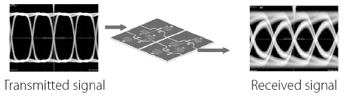
Figure 1: The eye diagram clearly shows the signal attenuation between the transmitted signal waveform and the received signal waveform. 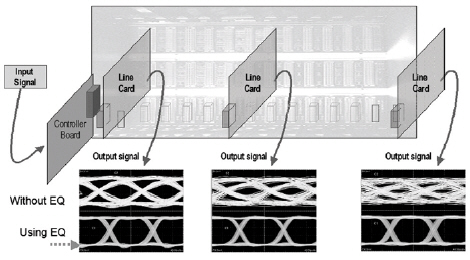
Figure 2: Proper equalization can successfully restore the attenuation superposition produced on the signal path. 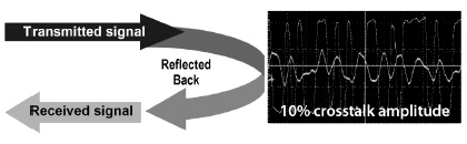
Figure 3: Even moderate crosstalk can affect signal integrity due to reflections.
Compared with traditional stock exchanges, digital asset trading platform not only matches transactions, but also plays the role of market maker and investment bank. The role of the market maker in the trading platform can increase the liquidity of the market, and the trading platform can earn the transaction price difference. The role of the investment bank of the trading platform is to provide services such as issuance and underwriting of digital currency, from which the trading platform collects money fees, or collects deposits in the form of community voting of the trading platform.
Discussion on Signal Integrity of High Speed ​​System
The 10Gbps rate suffers from discontinuity problems. It not only exists in a single device, but also exists in the electrical connection of the circuit board. Therefore, the PCB layout and the selection of the substrate material (such as FR4) will be affected at the same time. It seems that the neat, "clean" transmission signal at the receiver side will become completely unrecognizable, as shown in the eye diagram of Figure 1.