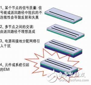
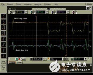
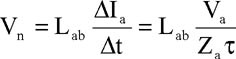
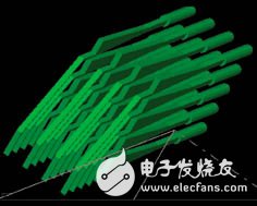
In high-speed circuit design, Chinese design engineers usually do not specifically understand the role of the connector's mutual inductance characteristics in improving signal integrity design. This article will explore the most difficult problem in connector design and selection: concurrent switching noise, and revealing concurrency The effect of switching noise on connectors and package specifications used in high performance systems. People always think that all the work in the system is done by IC, and of course the corresponding software. Passive devices like IC packages, boards, connectors, cables, and other discrete components can only reduce system performance, increase system size, and increase system cost. Therefore, the interconnection and selection and design of components in the system is actually to minimize the impact of these components on the system. Therefore, most IC designers usually attribute all parts of the system that are not connected (which are usually the contents of the PCB designer) to a general category of parasitic components. Figure 1: The four most important high-speed circuit problems When selecting an IC device, in addition to selecting the appropriate components, subsequent board layout work must comply with the following design rules: 1. PCB line with controlled impedance; 2. The signal delay on the branch line is less than 20% of the fastest signal rise time; 3. The discontinuity time delay is less than 20% of the fastest signal rise time; 4. Adjacent PCB lines have sufficient spacing to ensure signal crosstalk control is at an acceptable level; 5. Reasonable PCB layering design ensures that the medium between adjacent power and ground planes is thin; 6. There is a continuous signal return path below each signal line. Even if the PCB layout is done very well, things are still not that simple. Every component in a high-performance system needs to be optimised to ensure compliance with the overall system's cost, performance, and development schedule. The high-performance system design is a chain of interlocking links, each of which must meet the requirements to ensure that the entire system meets product performance specifications. How will other factors in the system affect system performance? Possible problems can usually be attributed to two types: timing problems and noise problems. Signal integrity includes both timing and noise issues, but the noise problem is more pronounced. Figure 1 shows four types of signal integrity issues caused by interconnects and components: 1. Signal quality of a single network; 2. Signal crosstalk between two or more networks; 3. Noise in the power distribution system; 4. External electromagnetic radiation of components in the system. Unless you pay special attention to it and the project begins to consider these issues, the above four types of problems will appear in high-speed products. This article explores the most difficult issues in the design and selection of connectors (including IC packages): simultaneous switching noise, and reveals the effects of concurrent switching noise on connectors and package specifications used in high performance systems. . Concurrent switching noise For connectors and IC packages, the high-speed performance requirements for switching noise are the most difficult to meet. Switching noise is a signal crosstalk, mainly due to the mutual inductance between adjacent loops (consisting of signals and return paths) in the connector and IC package. To minimize the amplitude of the switching noise, it must be ensured that the mutual inductance between adjacent signal path loops is less than an allowable maximum. Figure 2: Measuring concurrent switching noise in a BGA package. When a signal propagates through a connector or IC package, the wavefront of the signal (the component of the transition in the signal waveform) forms a current loop through the signal pin that couples and returns to the return pin of the signal. Each signal and corresponding return path can form a similar loop. There is a loop mutual inductance between the loops formed by any two signals and their return paths. When the current in one loop changes, the signal noise is induced in another loop that is stationary (no change in signal current). When a plurality of varying signal lines are concurrently switched, the noise coupled to the stationary loop by mutual inductance accumulates with each other, and is therefore referred to as "concurrent switching noise." Figure 2 shows the concurrent switching noise on a stationary signal line measured when five data lines are concurrently switched. In this example, the noise on the stationary signal line is caused by the mutual inductance between the stationary loop and all five varying loops. Mutual inductance calculation A simple model makes it easy to estimate the maximum allowable mutual inductance between two signal loops. Further discussion of how to calculate the mutual inductance between adjacent loops in the actual connector. When the signal passes through a pin pair of the connector, a sudden change in the signal current occurs at the wavefront of the signal over the varying signal path. The varying current causes voltage noise and is induced on adjacent stationary signal loops due to the mutual inductance between the two loops. The noise induced on this stationary signal line is called switching noise because it occurs only when the voltage or current is in the switching state. The voltage noise induced in the stationary loop can be approximated as: The meaning of the expressions is: Vn, noise in the stationary loop; Lab, the mutual inductance between the change loop and the stationary loop; ΔIa, the change in current in the change loop; Za, in the change loop and at rest The apparent impedance of the loop; Va, the signal voltage in the change loop; Δt is the rise time of the signal, indicating the speed of the current switch. The only thing that can be influenced by the choice of connector or IC package is the mutual inductance between the loops. The apparent apparent impedance of the signal in the loop is usually around 50 ohms. This impedance value is part of the system specification as the rise time and signal voltage. The allowable switching noise amplitude depends on the noise distribution. Switching noise should typically be less than 5% to 10% of the signal swing. Of course, the noise distribution depends on the engineer's design skills and who is responsible for selecting the connector or IC package. The negotiators of good signal integrity engineers are very clear: how difficult it will be to find a connector or package with low enough mutual inductance, so he will try to get a more relaxed mutual inductance indicator, and the result will inevitably lead to The specifications in other parts of the system are more stringent. You can start this estimation first by using the following values: First, you can use the following values ​​to start this estimation: Vn / Va = 5%, Za = 50 ohms, t = 0.5 ns, the maximum allowable mutual inductance value calculated by the above formula is 1.2n Figure 3: 3D solid model of the connector pins Determining the above application assumptions is equivalent to imposing constraints on the allowable mutual inductance values ​​between the signal paths of the connectors or packages. Of course, before weigh the time, cost, and product risk and implement resource allocation, good design engineers should use more sophisticated and comprehensive system-level simulation to see how much mutual inductance can ensure design success without causing system damage. Excessive burden. Therefore, the above estimate is only an initial expected value. In fact, the above estimate overestimates the allowable mutual inductance value because it is assumed that the noise on the stationary signal line is only caused by a signal change of an adjacent varying signal path. In actual situations, there may be multiple signal paths that change concurrently, and the signal path of each switch generates concurrent switching noise to the stationary signal line. Depending on the design of the connector, the actual allowable mutual inductance between the signal pins is typically only half to one-fifth of the above estimate. Is the mutual inductance value between the connector pin pairs or the package lead pair 1.2nH too large? Looking at a concrete example, we find that 1.2nH is actually a small value, and it is possible to reduce the value by doing a lot of hard work for the actual connector or package.
With a light output of up to 16,800 lumens, our Outdoor Led Wall Light Fixtures will light up any area to create a more secure environment. Outdoor Led Wall Pack is perfect for outdoor perimeter and area lighting. Features wide lateral spacing. And Outdoor Led Wall Light Fixtures will save you up to 85% on your energy bill. Bbier Outdoor Wall Lights come with a silicone gasket which PREVENTS LEAKAGE from the outside. It is also HEAT AND IMPACT RESISTANT. Comes in a standard dark bronze finish to match any area. Made of Glass or PC Lens. Glass will not degrade or change colors from sunlight exposure.
We uphold the highest standards for all our products by testing each product for optimal performance and safety. Bbier Outside Wall Lights are non toxic, unlike traditional HID wall packs, and will not fade over time, so you can enjoy a consistent high output light. The IP65 weatherproof rating ensures our Led Wall Pack can stand up to the elements. Outdoor Led Wall Light Fixtures is ideal for outdoor spaces such as building exteriors, parkings lots, street/alleyways, paraking lots and garages.
Outdoor Led Wall Light Fixtures Outdoor Led Wall Pack,Outdoor Led Wall Light Fixtures,Outdoor Wall Lights,Outside Wall Lights Shenzhen Bbier Lighting Co., Ltd , https://www.chinabbier.com