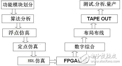
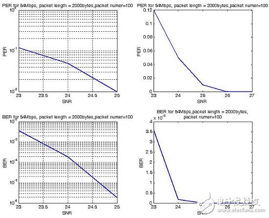
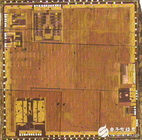
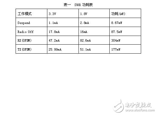
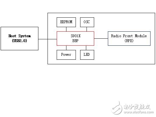
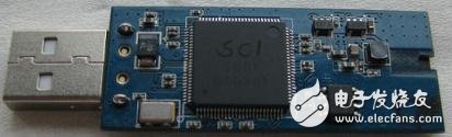
In 1999, the industry established the Wi-Fi Alliance to address the production and device compatibility issues of products that comply with the 802.11 standard. Wi-Fi is not only used in almost every smartphone currently sold, but also in almost all handheld game consoles, tablets, and laptops. There are Wi-Fi chipsets in a large number of new applications involving automobiles, digital cameras, e-book readers, Blu-ray devices and personal video recorders, as well as every device. As a result, market research firm In-Stat predicts that the annual shipment of Wi-Fi chipsets will exceed 1 billion units in 2012. At present, the development trend of Wi-Fi chips has the following development trends in addition to the IEEE 802.11b/g baseband chips with a maximum rate of 54 Mbps: Trend 1: Development in a high rate direction. These chips support an 802.11n standard that supports a minimum of 1 x 1 with a maximum speed of 150Mbps. The 802.11n chip with MIMO technology has a maximum rate of 300 Mbps or more and is mainly used for high-definition image transmission. It is worth noting that the support standard for high-rate chips will transition from IEEE 802.11n to IEEE 802.11ac (the frequency band below 6 GHz, the maximum rate). Up to 1Gbps) and IEEE 802.11ad (60GHz operating band, maximum speed up to 7Gbps). Trend 2: Low power consumption and low speed development. These chips emphasize low power consumption, low speed requirements, and a maximum rate of 2 Mbps. They only need to support the IEEE 802.11b standard, and there is a large market for industrial applications and IoT applications. Trend 3: Integration with other networks, such as integration with 3G and future 4G networks. The architecture of the Wi-Fi baseband chip is generally classified according to whether or not the processor is used: The first type is a full-hardware type, and no processor is used. The MAC (Medium Access Control) layer and the Phy (Physical Layer) of the entire chip are all implemented by hardware logic. The second type is semi-soft and semi-hard. The processor is used in the MAC layer, which is usually a MIPS core, and a small part uses the ARM core. The physical layer is implemented by hardware logic. The third is fully soft, this chip uses high-speed DSP, MAC and Phy are all implemented by software. These types have their own advantages and disadvantages, and are available on the market. In general, the first full hardware design is relatively difficult and processing speed is relatively fast. And because there is no processor, the cost will be relatively low. The third full-software type can be flexibly configured and upgraded. With the development of DSP's high speed, small area and low power consumption, the proportion of full software design will gradually increase. SCI baseband chip introduction S901 chip structure: The Wi-Fi baseband chip introduced in this paper is SCI's first generation Wi-Fi baseband chip. The process is 0.18 micron CMOS and the interface is USB 2.0 interface. Belonging to the first full hardware type mentioned above, the internal MAC and PHY of the chip are all implemented by hardware. The chip structure is shown in Figure 1: The entire baseband chip is divided into a USB interface part, MCU, MAC, PHY, ADC/DAC. The built-in MCU executes the USB firmware program. Figure 1: SCI first generation baseband chip S901 structure Development process: The whole design adopts a top-down design method. The chip architecture is first designed, and the chip is divided into three main parts: driver, MAC, and Phy. The design of the driver part is carried out by the software engineering design method; because the driver runs on the PC side, it has to interact with the hardware (network card), so the communication message must first be developed. The design of the MAC part is followed by analysis of the protocol, hardware and software partitioning, to determine which are done by hardware, and those done by software. The physical layer involves more communication algorithms, such as frame synchronization algorithm, frequency synchronization (coarse frequency synchronization, fine frequency synchronization), channel estimation, code decoding, modulation and demodulation, etc., and the simulation determination algorithm needs to be performed first. The development process of the entire physical layer is shown in Figure 2. Figure 2: Physical layer development process Simulation: During the development process, the physical layer algorithms are subjected to rigorous simulation, and the simulation results meet the design specifications before the HDL design begins. Figure 3 below shows the 54 Mbps simulation results of OFDM modulation and demodulation. Standard regulations: PER "10%, SNR" 25@54Mbps. Figure 3: OFDM 54Mbps simulation results. Technical features: The baseband part does not use the processor to reduce the chip area and improve the processing speed; the on-chip MCU is responsible for executing the USB firmware program and performing the MAC layer and physical layer configuration; the physical layer core algorithm adopts a proprietary patent algorithm; supports WAPI, IEEE802.11i encryption standard, multiple encryption methods are seamlessly integrated; the part with low real-time MAC requirements is implemented by software, which is easy to upgrade and maintain. Chip area: The logic unit of the chip is: 863K gates (MAC+PHY+USB+MCU) The MEMORY size is 271Kbits. The Die size at 0.18um is: 23mm2 (including analog parts such as ADC/DAC/LDO). The S901 chip layout is shown in Figure 4. Figure 4: S901 chip layout. Chip Power Consumption: The power consumption of the entire baseband including the internal ADC/DAC is shown in Table 1. Table 1: S901 power consumption table. Wireless network card design based on SCI Wi-Fi baseband chip Structure and main technical indicators of SWM9001 Wi-Fi wireless network card SWM9001 is a Wi-Fi wireless module based on the RF chip S103 and the baseband chip S901 with independent intellectual property rights of Suzhou Zhongke Semiconductor Integrated Technology R&D Center Co., Ltd. (Linxin Integration). The product was acquired on September 30, 2011. -Fi Alliance product certification, certification number is WFA12939. The wireless module is the first product in China to be certified with its own intellectual property Wi-Fi chip design. Figure 5 below is a structural diagram of the network card, and Figure 6 is an outline drawing of the network card. Figure 5: The SWM9001 network card is composed. Figure 6: SWM9001 shape. The main indicators of the SWM9001 NIC are as follows: * Comply with IEEE802.11b/g/e/h/i standard and support WAPI encryption standard; * Encryption standard: 64/128/152bitWEP, WPA/WPA2/WPA-PSK/WPA2-PSK, WAPI; * Interface: USB2.0; * Transmission rate: 6/9/12/18/24/36/48/54Mbps@ 802.11g; 1/2/5.5/11Mbps @802.11b; * Modulation method: BPSK/QPSK/16QAM/64QAM@11g; DQPSK/DBPSK/DSSS/ ; * Receive sensitivity: -71dBm@11g, 54M; -90dBm @11b, 11M; * Driver: Window ME/SE/XP/2000/Vista/Win7, Linux 2.6.28and Android 2.1/2.2/2/3; * Transmission distance: indoor 100 meters, outdoor: 300 meters. Applications: Smart Integration provides a complete solution (schematic, PCB, BOM, driver) for this reference design, with product design taking into account power, stability, ease of use and scalability. Performance is at the forefront of similar products, and the price has a considerable competitive advantage. The Wi-Fi wireless module can be applied to PC wireless network cards, wireless video transmission, home wireless gateway, industrial data wireless transmission and other occasions. SWM9001 wireless network card design skills and considerations The circuit of the wireless network card mainly includes a radio frequency front module (FEM), a radio frequency module (RF), a baseband chip and a power supply part. The matters needing attention in the design are mainly the electromagnetic compatibility and interference problems of the RF front-end module (FEM) and the RF module (RF): 1) FEM filter capacitor 100uF; Because the PA part of the FEM operating current accounts for a large proportion, a large-capacity filter capacitor is required; 2) The power input of the Wi-Fi RF unit needs to be connected to a magnetic bead to suppress high frequency noise and spike interference on the power line and improve the transmission accuracy; 3) The active crystal oscillator (40MHz) clock line width must be no less than 8mil, preferably on the top layer or bottom layer (Bottom layer); do not walk 40MHz clock in the inner layer, the shorter the clock line, the better, if needed For perforation, the recommended hole size is 30 mil outer diameter and 15 mil inner diameter; 4) The recommended 50 ohm impedance linewidth on a four-layer PCB is 12 mils; the RF section must retain the full ground plane; 5) When laying out the PCB, the DC-DC is preferably close to the USB interface; the farther the clock line is from the 50 ohm impedance line, the better.
Strong and durable
Hidden design
Data Cable Wiring,Original Data Cable,Computer Transfer Cable,Line Data Charging Cable Guangzhou HangDeng Tech Co. Ltd , https://www.hangdengtech.com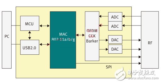
Aluminum alloy plug, TPE cover
Ultrasonic welding pressure
Close fitting, firm resistance to fall
Strong and durable
Priority TPE
It's hard to break even if you stretch multiple times
Stretching or shrinking only one end can easily to damage the components and cause jamming
No winding
Stretch when used, shrink when not used
Five lengths
Each pause is a length, suitable for multiple occasions
Notice
Both cables are stretched at the same time
Do not stretch unilaterally