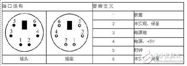
This example demonstrates how to control the keyboard, LCD, and RS-232 interface on the Red Hurricane II Xilinx development board using Verilog programming. The system is designed to capture input from a PS/2 keyboard and display it either on the onboard LCD or through the RS-232 port to a PC connected via HyperTerminal. This provides a practical way to interact with hardware using digital logic design. The goal of this example is for the reader to gain hands-on experience in the following areas: The PS/2 interface uses a two-way synchronous serial communication protocol. Data is transmitted one bit at a time over the data line, synchronized by the clock signal. Each bit is sampled on the falling edge of the clock pulse. The host (in this case, the FPGA) has priority over the bus and can interrupt the keyboard by pulling the clock line low at any time. To implement this in Verilog, we first need to understand the structure and pin functions of the PS/2 interface. Table 1 shows the pin definitions for the PS/2 port. Table 1: PS/2 Port Structure and Pin Definition As shown, the PS/2 port only has one data line. To distinguish multiple keys, the keyboard uses scan codes. These are unique codes sent when a key is pressed or released. There are two types of scan codes: "make codes" for key presses and "break codes" for key releases. Some keys also use extended scan codes, which begin with an "E0" prefix. When a key is pressed, the keyboard sends a make code. When the key is released, a break code is sent. For extended keys, the break code starts with "E0F0". This helps the host identify the exact key being used. Each keyboard transmission consists of 11 bits: one start bit (0), eight data bits (LSB to MSB), one parity bit, and one stop bit (1). This is illustrated in Figure 2. Figure 2: PS/2 Serial Protocol Here is a step-by-step guide to implementing the PS/2 keyboard interface in Verilog: Once the program is running, the characters typed on the keyboard will be displayed on the LCD screen of the development board. Alternatively, the same input can be sent through the RS-232 interface to a PC, where it appears in HyperTerminal. This example offers a clear understanding of how to interface external devices with an FPGA using Verilog. Customized Solar Panel, 100watt solar panel,200watt solar panel, big solar panel, high efficiency high quality solar modules
different power customized and OEM logo customized solar panel
Customized solar panel data
Customized Solar Panel,Noncrystalline Solar Panel Module,Cheap Price Pv Solar Module,Solar Photovoltaic Pv Panel PLIER(Suzhou) Photovoltaic Technology Co., Ltd. , https://www.pliersolar.com
Principle Introduction

solar cell type
mono crystalline half cut cell
power range
50watt to max 700watt
size and weight
different size and different weight if the power is different
solar panel type
monofacial or bifacial
solar panel color
sliver or black
Product details and pic


Verilog-based PS/2 interface control program
1. Main Content of the Example