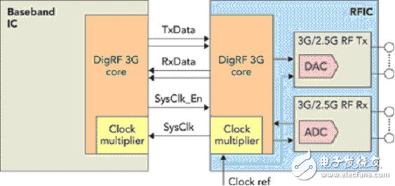
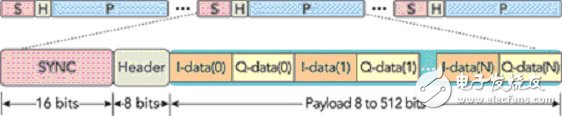
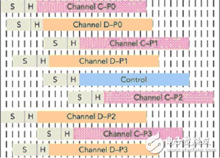
DigRF is set to replace the traditional methods of data communication between RF and baseband semiconductor components, such as analog signaling and proprietary digital interfaces (either parallel or serial). The MIPI (Mobile Industry Processor Interface) Alliance is working on replacing various I/Q (in-phase/quadrature phase) signaling interfaces with a standardized, packet-based digital serial interface through the DigRF (digital radio frequency) standard. A dedicated working group within the MIPI Alliance has developed the DigRF specification for 2.5G and 3G handsets, with future versions expected to support higher data rates required by 4G standards. By adopting the DigRF standard, designers gain greater flexibility in selecting components. For instance, they might source an expensive baseband IC from one supplier while purchasing RF, power management, and other modules from different vendors. However, this increased flexibility also introduces challenges, especially when it comes to testing strategies due to the complex nature of general-purpose systems. During RF reception testing, the primary goal for engineers remains consistent with previous technologies: capturing I/Q data, applying custom digital signal processing algorithms, and recording results to determine device qualification. However, DigRF devices may introduce significant overhead during production testing. Engineers must find ways to reduce this overhead to ensure efficient and effective automated test systems. Understanding the DigRF interface is essential for effective testing. The DigRF 3G standard defines the minimum number of signals needed for an interface, requiring only six wires in a basic phone configuration (Figure 1). The RxData/TxData signal carries I/Q data along with control and status messages in a packet format. Figure 1. A basic DigRF phone setup uses just six wires. Data transmitted via DigRF is encapsulated in packets, each consisting of three main parts: sync, header, and payload (Figure 2). Each packet begins with a 16-bit synchronization sequence, which helps the digital receiver align the real-time strobe phase for each frame. The next 8 bits form the header, defining the payload’s role and content. This header includes three parts: 3 bits for the payload size, 4 bits for the Logical Channel Type (LCT), and 1 bit for the Clear to Send (CTS) signal. Figure 2. The DigRF 3G data frame starts with a 16-bit sync sequence, followed by an 8-bit header and I/Q data. The payload size varies across different packets, leading to varying levels of coding overhead. The LCT determines what type of data is included—whether it's control data or I/Q data. The CTS allows the RF device to manage the data stream from the baseband during transmission. The remaining N bits in the frame carry the actual data being transmitted. For example, in non-diversity mode, the RxData frame may use a 256-bit payload containing alternating I and Q data. DigRF 3G supports three timing modes based on the type of RF information being transmitted (Table 1). It also supports three common reference clock frequencies (19.0 MHz, 26.0 MHz, and 38.4 MHz), which are sent to the baseband via the SysClk signal. Regardless of the speed mode, the DigRF processor manages the data stream using a local FIFO buffer, which can produce unpredictable timing when transmitting frames. One of the main challenges in testing DigRF protocol devices is managing the uncertainty in the RxData packet during RF reception testing. Multiple levels of uncertainty exist in the synthesis state of the RxData signal, including phase timing, frame timing, frame type, and the content of the payload. The 312 Mbps data rate is derived from a 1/4 division of a 1248 MHz master clock (typically generated by a PLL). In a production test system, the clock input to the device should be provided by the RF instrument, taking into account the impact of phase noise on the RF front end. The starting phase of this clock source is usually uncontrollable compared to a normal digital subsystem, making the DUT’s input clock phase unknown. This uncertainty, combined with the phase generated by the PLL multiplier/divider, leads to unpredictable RxData output timing, even across multiple devices in a test configuration. A production tester must have the capability to maintain the operation of the digital subsystem while making necessary hardware and DUT adjustments between tests. This ensures that the tester can maintain strobe timing relative to the DUT output, avoiding the need for phase retuning during actual operations, thus saving valuable test time. Another critical challenge is handling the multi-level uncertainty in packet transmission performance. As shown in Figure 3, during each RF receive test of the DUT, the tester cannot predict when a packet will be transmitted, what type of packet it will be, or whether it matches the expected type (e.g., an active control status message from the RFIC). 86inch Multimedia All-in-One PC Touch the screen, Multi-touch panel,Intelligent touch display Jiangsu Qilong Electronic Technology Co., Ltd. , https://www.qilongtouch.com