Bluetooth Hat Headphones are a combination of fashion and technology, so you can listen to music without wearing extra headphones. Bluetooth Stereo Headphones bring you sound quality, style and comfort.The latest Blutooth V5.0 technology: Easily and quickly work with mobile phones, tablets and other Bluetooth music devices, with a wireless range up to 33 feet. To answer and hang up calls, you can operate directly on your hat without using your phone. Built-in rechargeable lithium-ion battery, about 6 hours of call/play time, 2.5 hours of charging time, 60 hours of standby time, so you have less charging time and more working time. The hat can be completely washed after taking off the headphones.
Bluetooth Hat Headphones Wireless Bluetooth Headset,Bluetooth Earphone,Bluetooth Hat Headphones,Winter Hat With Bluetooth Headphones Shenzhen Linx Technology Co., Ltd. , https://www.linxheadphone.com
Introduction The reliability of the 1-Wire network depends to a large extent on the performance of the communication drive circuit used between the host and the 1-Wire slave device. This article introduces a 1-Wire host terminal interface, using fine impedance matching and "intelligent" (software control) strong pull-up methods to ensure that the network can work reliably in the light load to heavy load range, and the communication distance can be Up to 500m. For guidelines on creating reliable 1-Wire networks, see Application Note 148.
Circuit description The network driver (Figure 1) consists of a pull-down part (Q1, R1, C1, R5) and a pull-up part (Q2, R2, C2, R6). Transistor Q3 and the surrounding components (C4, R7) form a strong pull-up circuit, which can provide additional power for devices such as EEPROM and temperature sensors. This article does not discuss the "strong pull-up" function. At any time, at most one of the three transistors is in the on state; when 1-Wire is not communicating ("idle" state), these three transistors are not on. 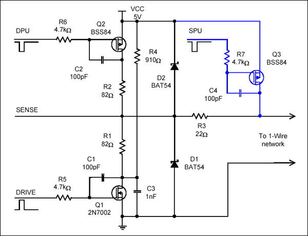
Figure 1. Schematic diagram of the driver
The series circuit of R4, R1, and R3 provides a standard 1-Wire pull-up to VCC. In this circuit case, the total pull-up resistance is approximately 1kΩ. When the 1-Wire line is idle, this impedance appears on the line. Because R4 is connected to the drain of Q1, current flows through this resistor when Q1 is on, but it does not affect the low-level voltage of the 1-Wire bus. The speed at which the 1-Wire bus voltage rises to 5V is determined by the resistance value of R4 + R1 + R3 and the load of the 1-Wire network. It is not recommended to reduce the resistance of R4, otherwise it will cause the low voltage of the 1-Wire bus to rise, which is not what we expected. By turning on Schottky diodes D1 and D2 to GND and VCC, respectively, ESD strikes and coupled signals from adjacent cables are suppressed. Resistor R3 limits the ESD current and protects D1 and D2.
One of the most obvious features of this driver is that it can be strictly terminated on the host side with the 1-Wire cable. It is recommended to use Category 5 unshielded twisted-pair data cables in the 1-Wire network, whose characteristic impedance is about 100Ω. When Q1 or Q2 is turned on, the bus terminal matching is achieved by the series connection of R3 and R1 or R2, respectively. C3 and R1 and R3 are connected in series to provide an AC-coupled terminal match for the online response pulse. In order for the driver to adapt to different characteristic impedance cables, R1 and R2 need to be adjusted accordingly.
When the corresponding transistors of the three parts of the driver are turned on, the slew rate is controlled. When the driver turns the 1-Wire bus low (for example, a certain timing or the start point of a reset pulse), R5 and C1 control the falling slope; R6 and C2 limit the slew rate when the dynamic pull-up signal becomes active; R7 and C4 limit the slew rate of strong pull-ups. The time constant of all three parts is 0.5µs, and the slew rate is approximately 4V / µs. For details and oscilloscope waveforms, please refer to the Performance Examples section.
If the circuit works ignoring the strong pull-up circuit (Q3, R7, C4), the driver requires three signals to be connected to the monitoring microcontroller, these signals are DRIVE, DPU and SENSE. DRIVE is an active high signal, which enables 1-Wire communication by turning on Q1. DPU is an active low signal used to activate the dynamic pull-up transistor Q2. SENSE is a direct connection signal between the 1-Wire circuit and the input port of the microcontroller. The 1-Wire ground is shared with the driver / microcontroller GND. In order to carry on 1-Wire communication, must send out the appropriate DRIVE signal and DPU signal, and read 1-Wire bus signal through SENSE input port in the appropriate time. There are four kinds of waveforms in 1-Wire communication, they are reset / online response detection sequence, and three kinds of communication slot waveforms.
The reset / online response pulse detection sequence 1-Wire communication process starts with a reset pulse, followed by an online response pulse, the waveform is shown in Figure 2. When a reset pulse needs to be issued, the DRIVE signal should go high and stay from A to B (see Figure 2). From point A, the voltage of 1-Wire gradually drops to 0V. At point B, the DRIVE signal is released. Unless the 1-Wire device pulls the bus low to generate an interrupt signal (see DS1994 / DS2404 data sheet, interrupt type 2), the 1-Wire voltage begins to rise. In order to handle this interrupt correctly, the 1-Wire must be resampled from point C until the 1-Wire state at point D becomes a logic high level. Shortly after point D, the dynamic pull-up DPU signal becomes active (point E), the 1-Wire bus will be pulled to 5V at a faster rate, and the dynamic pull-up ends at point F. Assuming that there is a 1-Wire device on the bus, it will issue an online response pulse, starting at point G and ending at point I. Somewhere between G and I (point H), the 1-Wire state is sampled to determine whether a 1-Wire device is present. After the online response pulse ends, the 1-Wire voltage starts to rise to 5V. At point J, the 1-Wire logic state must be sampled again to determine whether a Type 1A interrupt signal has occurred (see DS1994 / DS2404 data sheet). When there is no interrupt signal, the logic state is high, and the dynamic pull-up signal from point K to point L becomes active again to ensure that the 1-Wire bus voltage rises to 5V, as shown in Figure 2. When an interrupt signal is generated, the state detected at point J will be logic 0, and the next round of repeated sampling process will begin, just like the end of the reset pulse (such as returning to point C to continue sampling). If there are other 1-Wire devices on the bus, in addition to the device that issued the interrupt, they will treat the interrupt pulse as a reset pulse, and then send an online response pulse as a response. (For example, when the J point is reached for the second time, the logic state of 1-Wire is high, as shown in Figure 2). In any case, the reset / online response pulse detection ends at point M and is also the beginning of the next time slot. 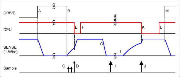
Figure 2. Timing of reset and online response pulses
Table 1. Recommended time values ​​for reset / online response pulse detection sequence A to B B to C D to E E to F E to H H to J J to K K to L L to M 480µs 0 to 2µs 0 to 2µs 8µs 72µs 240µs 0 to 2µs 60µs > 2µs
Sampling point H must be selected within the response pulse window. The online response pulse window is determined by the time of the fastest and slowest 1-Wire device online response pulse. The data window specifies the length of this window as tMSP. After the reset pulse ends, when the 1-Wire device detects a logic high level, it marks the beginning of tMSP. The reference point in Figure 2 is approximately point E. The length of time between A and C is equal to the sum of tF (fall time) and tRSTL (low reset time). When a type 2 interrupt occurs, the effective reset time length is the sum of the duration from A to B and the duration of the interrupt pulse (see DS1994 / DS2404 data sheet). The time from E to M is called the high-level reset time tRSTH. The data sheet specifies tRSTL and explains how to determine the minimum tRSTH value, but there is no maximum value for tRSTH.
Communication time slot write 0 time slot write 0 time slot is used to transfer bit 0 in the 1-Wire bus, the corresponding 1-Wire waveform is shown in Figure 3. When you need to write a 0 time slot operation, the DRIVE signal must first become an active level state and continue for a period of time, the corresponding points in the figure are points A and B0. From point A, the voltage of the 1-Wire bus slowly drops to 0V. When the DRIVE signal is released at point B0, the 1-Wire bus voltage begins to rise. Shortly after point B0, the dynamic pull-up DPU becomes active (point C0), and the 1-Wire bus will be pulled to 5V at a faster rate. The dynamic pull-up signal ends at point D0, and the next time slot or reset / online pulse detection sequence will immediately follow point E. 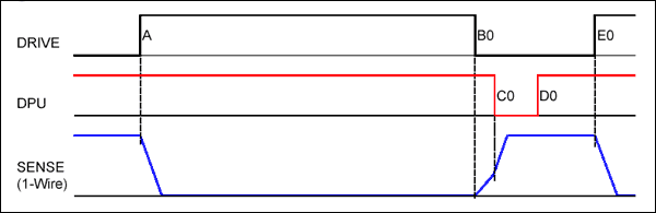
Figure 3. Write 0 time slot
Writing a 0 time slot does not require sampling of the data line, so Figure 3 does not indicate any sampling points, but it is also allowed to sample the 1-Wire bus at the same time point in the read time slot (Figure 4 or Figure 5), but obtain The sampling logic state of will always be 0, indicating that the circuit is writing a 0 to the 1-Wire bus. The duration from A to C0 is equal to the sum of tF (fall time) and tW0L (write 0 low time), and the time from C0 to E0 is called the recovery time tREC. The data sheet specifies the minimum value of tW0L and tREC. The time from A to E0 is called the slot period tSLOT.
Table 2. Recommended time values ​​for writing 0 time slots A to B0 B0 to C0 C0 to D0 A to E0 60µs 2µs 16µs 80µs
Write 1 / Read 1 time slot Write 1 time slot is used to transfer bit 1 from the 1-Wire bus. The corresponding 1-Wire waveform is shown in Figure 4. Actually, the operation waveform of reading bit 1 from the 1-Wire bus is the same as the writing waveform of the writing 1 operation. Therefore, the writing 1 operation and the reading 1 operation are discussed as one case. To generate a write 1 or read 1 time slot, first turn the DRIVE signal at point A and continue until BR. Starting from point A, the 1-Wire bus voltage slowly drops to 0V. At the BR point, the DRIVE signal is released. Whether it is a read 1 operation or a write 1 operation, the 1-Wire bus voltage starts to rise. Sample the 1-Wire bus at CR. Since the bit read is 1, the dynamic pull-up DPU will immediately become active and continue from D1 to E1. This will cause the 1-Wire bus voltage to rise to 5V at a faster rate. The next time slot or reset / online response pulse detection sequence can start from point F1. 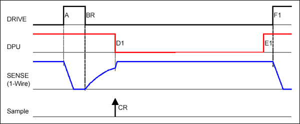
Figure 4. Write 1 / Read time slot (Read 1)
The sampling point CR must fall within the sampling window of the host, determined by the fastest 1-Wire device response time. This time window is called tMSR in the data. After the time slot starts, the 1-Wire device detects the logic low level as the starting point of tMSR. This reference point in Figure 4 is approximately point A plus the pulse fall time tF. The duration from A to BR is equal to the sum of tF (fall time) and tRL (read low time). The data materials specify tRL (equal to tW1L) and tMSR, and the time from A to F1 is the time slot cycle time tSLOT.
Table 3. Recommended write 1 / read time slot (read 1) time values A to BR A to CR CR to D1 D1 to E1 A to F1 9µs 18µs 0 to 2µs 60µs 80µs
Read time slot (read 0) The read 0 time slot is used to read bit 0 from the 1-Wire bus. The corresponding 1-Wire waveform is shown in Figure 5. When the read time slot operation is required, the DRIVE signal must first become an active level state and last for a period of time, corresponding to points A and BR in the figure. From point A, the voltage of the 1-Wire bus slowly drops to 0V. To send bit 0, the 1-Wire device needs to pull 1-Wire low, from point A to the end of BR. In this case, at the beginning of the 1-Wire bus, the 1-Wire master pulls the voltage low, and at the BR point, the master pulls down to end, and then one or more 1-Wire devices present on the bus continue to turn the 1-Wire bus voltage. Maintain a logic low state. Sample the 1-Wire bus at the CR point. Since the bit read is 0, the 1-Wire bus will be resampled. At point D0, the 1-Wire device stops pulling down, and the 1-Wire bus voltage begins to rise. Sampling is performed again at E0 to determine whether the bus is already at a logic high state, and the dynamic pull-up DPU becomes active, and the 1-Wire bus voltage starts to rise to 5V at a faster rate. The active state of the dynamic pull-up DPU continues from F0 to G0. The next time slot or reset / online response pulse detection timing can start from H0. 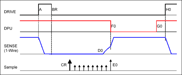
Figure 5. Read time slot (read 0)
The selection of CR sampling points is the same as when writing 1 / read time slots, and the subsequent repeat sampling interval should be as short as possible within the allowable range of the microcontroller and software. The time from A to H0 is the slot cycle time tSLOT.
Table 4. Recommended read slot (read 0) time values
Application Considerations The signal structure for controlling this advanced 1-Wire network driver is relatively complex. However, the algorithm is relatively intuitive, so this driver is usually implemented in software, using a fast enough microcontroller to generate real-time signals. The flow chart below will help users to use any familiar microcontroller to meet the requirements to realize the driver. In order to generate appropriate timing signals, the execution time of each command at the selected crystal frequency must be considered. Software flow chart A to BR A to CR E0 to F0 CR to G0 A to H0 9µs 18µs 0 to 2µs 60µs 82µs 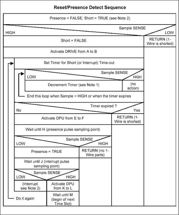
Note 1: If the timer is only used as a counter instead of a real-time timer, a down counter must be used. The timer should expire after 5000µs.
Note 2: Presence and Short are logical variables used to report the results of reset / online response pulse detection time slots to advanced programs. Since there is only one 1-Wire chip (DS1994 / DS2404) that can generate interrupts, and using interrupts will greatly reduce the effective speed of the 1-Wire network, interrupts are not reported as variables. 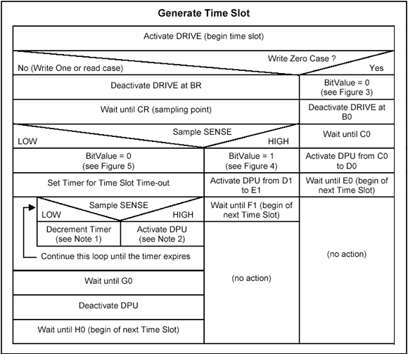
In this flowchart, a logic input variable is used to control whether a write 0 time slot or a read 0 time slot is generated. Writing 1 time slot is the same as reading 0 time slot. The bit variable BitValue is used to report the result of the time slot execution to the superior program.
Note 1: If the timer is only used as a counter instead of a real-time timer, a down counter must be used. The timer should expire after 45µs.
Note 2: According to this flowchart, before the timer stops, the DPU signal will be repeatedly asserted. If the signal is already in the active state, the activation operation will not affect it, so the DPU signal that is already in the active state is allowed to be activated. If necessary, you can also check whether the DPU signal is valid. If the DPU signal is valid, you do not need to activate it again when executing the program.
Performance Examples The oscilloscope waveform of the 1-Wire signal generated by the driver discussed in this article is shown on the following page. When verifying the signal, especially at the farthest end of the cable, a differential probe must be used. The reference ground of the probe is suspended, otherwise the ground of the probe will bypass the 1-Wire reference ground, thereby changing the topology of the system. If you cannot provide a differential probe, you must isolate the oscilloscope ground from the bus ground through a transformer or a battery-powered oscilloscope. You can choose one of two methods to disconnect the safety ground of the oscilloscope power cable.
Oscilloscope waveform 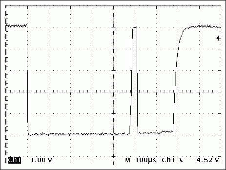
Reset / online response pulse detection time slot (Figure 2) 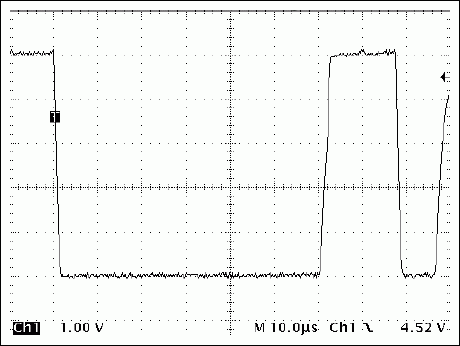
Write 0 time slot (as shown in Figure 3) 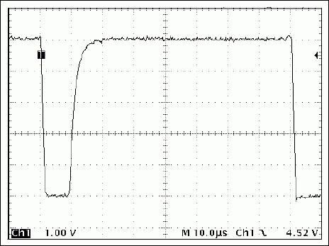
Write 1 / Read 1 time slot (as shown in Figure 4) 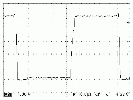
Read 0 time slot (as shown in Figure 5) 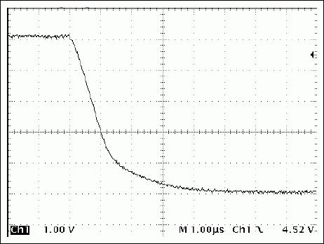
Falling edge signal at the end of 300m cable 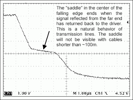
The same falling edge signal seen near the end of the 300m cable

Excellent performance 1-Wire network driver
Abstract: This article introduces a microcontroller-based 1-Wire® host interface suitable for small-, medium-, and large-scale 1-Wire networks. Using fine impedance matching and "intelligent" (software control) strong pull-up, slew rate control and other methods to ensure reliable operation of the network. This article gives a software flow chart to help users use any suitable microcontroller to generate the correct reset pulse, online detection, write "1", write "0" and read the 1-Wire timing of the time slot. The oscilloscope test curve illustrates the time characteristics of the driver and the influence of the transmission line during long-distance communication.