A Simple 1-Wire DAC
Abstract: ConnecTIng the outputs of a 1-Wire addressable switch (DS2408) to a resistor network allows the 1-Wire interface to control a simple DAC. This idea is illustrated by the presentaTIon of an LED-brightness controller.
A similar version of this arTIcle was published on September 29, 2009 on the Planet Analog website.
Among devices available with a 1-Wire interface, the best known are memories, temperature sensors, battery monitors, and addressable switches. One-Wire ADCs are also available, but no 1-Wire DACs. You can, however, build a simple 1 -Wire DAC using addressable switches.
The circuit (Figure 1) consists of a mulTI-channel 1-Wire addressable switch (DS2408, U1), a current mirror (Q1, Q2), and a resistor network (Rα, Rβ, Rγ, Rδ, RX). U1's open -drain output transistors (P0-P3) either conduct (logic 0) or present a high impedance (logic 1). If the logic state of an output port is 0, then current flows to ground through the resistor connected to that port.
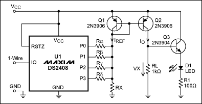
Figure 1. This 4-bit DAC is controlled by a 1-Wire interface. (DS2408 outputs P4 to P7 are not used.)
IREF is calculated as follows:

As explained in the Reference¹, the current IO is described by equation (2):

where VA represents the early voltage of Q2 and β is the current gain, assuming Q1 and Q2 have identical characteristics. For VCB values ​​from 4.3V to 0.2V and typical values ​​for VA (20) and β (180), the mirror ratio MR ranges from 1.20 (high VCB, low current) to 1.00 (low VCB, high current).
The DAC's analog output voltage (VX) is
| VX = IO × RL = MR × IREF × RL | (Eq. 3) |
When none of the output ports are asserting logic 0, IREF is determined by RX:
| IREF0 = (VCC-VBE (Q1)) / RX | (Eq. 4) |
IREF0 generates the offset voltage VX0:
| VX0 = MR × IREF0 × RL | (Eq. 5) |
Inserting (4) in (5) and solving for RX yields (6), which lets you calculate the RX value corresponding to a desired offset voltage:
| RX = RL × MR × (VCC-VBE (Q1)) / VX0 | (Eq. 6) |
With P0 assigned to the DAC's least-significant bit (LSB), the resistor Rα determines ΔVX, which is the voltage increment between steps. Substituting ΔVX for VX0 in equation (6) yields (7), which lets you calculate Rα:
| Rα = RL × MR × (VCC-VBE (Q1)) / ΔVX | (Eq. 7) |
Because P1 has twice the weight of P0 in a binary system, Rβ must conduct twice as much current. Consequently, Rβ = Rα / 2. For the same reasons, Rγ = Rα / 4 and Rδ = Rα / 8. For these conditions the maximum value of VX is
| VXMAX = VX0 + 15 × (VCC-VBE (Q1)) / Rα × RL × MR | (Eq. 8) |
Example 1: Full-Range DACTable 1 explains the choices for input values. Inserting these values ​​in equations (6) and (7) yields RX = 94.6kΩ and Rα = 18.92kΩ. Given the value Rα = 18.92kΩ, the other (non -standard) values ​​are Rβ = 9.46kΩ, Rγ = 4.73kΩ, and Rδ = 2.365kΩ. To get closer to E24 standard values ​​(5% tolerance), multiply each one with a factor ~ 1.05, yielding RX = 100kΩ, Rα = 20kΩ, Rβ = 10kΩ, Rγ = 5kΩ, and Rδ = 2.5kΩ. Changing all resistors by the same factor has little effect on the result, and the reduction in IREF is compensated by the increased value of RL, leaving VX unaffected.
Table 1. Input Values ​​for the Full-Range DAC
| Parameter | Explanation |
| VCC = 5V | Maximum voltage for the DS2408 |
| VX0 = 0.05V | Design objective |
| ΔVX = 0.25V | Design objective |
| VBE (Q1) = 0.7V | Simplification |
| MR = 1.1 | Center of the 1.00-to-1.20 MR range |
| RL = 1kΩ | To ensure operation with high current gain |
Example 2: LED-Brightness ControlIn Figure 1, the analog output voltage VX controls the light intensity of an LED. Q3 functions as an emitter follower that minimizes the load on VX, and R1 limits the LED current. Assume that the LED voltage drop is 1.9V when ON, and that VBE of Q3 is 0.7V. To keep the LED OFF, VX must be less than 2.6V, ie, VX0 = 2.5V. To avoid Q2's VCE saturation range, the voltage swing at VX must remain below 2V. This condition demands that ΔVX ≤ 2V / 15, ie, ΔVX = 0.125V. Otherwise, the input values ​​of Table 1 apply.
Repeating the calculations of equations (6) and (7) yields RX = 1.892kΩ, Rα = 37.84kΩ, Rβ = 18.92kΩ, Rγ = 9.46kΩ, and Rδ = 4.73kΩ. Increasing these resistor values ​​by ~ 5% gets you closer to the standard values: RX = 2kΩ, Rα = 40kΩ, Rβ = 20kΩ, Rγ = 10kΩ, and Rδ = 5kΩ.
The circuit of Figure 1 is simple and efficient, but its weak spot is the current mirror. The mirror ratio varies with VCB (Q2), and both the Early voltage VA and the current gain β change with the collector current. Discrete transistors introduce further imprecision. Using 5% resistors, the actual measurements of VX were within ± 10% of the calculated values.
You can improve the current mirror by replacing Q1 and Q2 with a transistor array, or a dual transistor such as the BCV62. (The improved current-mirror designs described in Reference [1] require a third transistor.) Though shown for four switches, this concept can be extended to use all eight ports of U1. Note that this approach increases only the resolution, and not the accuracy or the output-voltage range.
SMD Buzzer
Smd Buzzer,Smd Piezo Buzzer,Smd Micro Buzzer,Smd Magnetic Buzzer
NINGBO SANCO ELECTRONICS CO., LTD. , https://www.sancobuzzer.com