Abstract: Taking DALSA's CA-D7-1024T digital CCD camera as an example, the interface signals and timing relationships of the digital CCD camera are discussed in detail; the key technology of the digital CCD camera image transmission card is studied, and the circuit principle of the transmission card is introduced And the realization method of each part. With the development of CCD technology, new high-frequency, digital new CCD cameras are constantly appearing. The digitization of the output of the CCD camera simplifies the interface design between the camera and the transmission and acquisition system, making the digital CCD camera more and more a detector in real-time PCI control, data acquisition, graphic image processing, remote sensing telemetry and other systems. This kind of CCD camera mostly adopts frame transfer type architecture, with fast conversion speed, high quantization accuracy and high quantum efficiency. Accurate understanding of the camera's interface signals and their timing relationship, mastering the principles and implementation methods of their image data transmission cards, can greatly broaden the application field of digital CCD cameras and increase the flexibility of application systems. 1 Digital CCD camera and its interface technology In this system, the CA-D7-1024T digital CCD camera produced by DALSA is used. The camera is a frame transfer type CCD camera with a spatial resolution of 1024 × 1024 pixels, a single pixel size of 12 μm × 12 μm, and a 100% fill factor. Inside the camera, technologies such as correlated double sampling (CDS) and vertical anti-halation (VAB) are used to greatly improve the imaging quality of the camera. The camera outputs sampled and quantized data with a quantization accuracy of 12 bits, a maximum frame rate of 8.4 Hz, and an electronic shutter. The camera is composed of CCD image sensor, driver, timer, A / D conversion and other modules. The interface signals are divided into two categories: user bus interface signals and data bus interface signals. · EXSYNC? Trigger frame readout signal is a necessary signal. When EXSYNC is fixedly connected to low level, the camera outputs image data at the maximum frame rate; when EXSYNC alternates between positive and negative, its falling edge triggers frame reading. · PRIN? Pixel reset signal is an optional signal. The pixel is reset (discharging the capacitor that accumulates charge) between the two EXSYNC actives, thereby shortening the effective exposure time. PRIN is active low and effective exposure begins on its rising edge. If PRIN is fixedly connected to a high level, the integration time is maximum; if PRIN is fixedly connected to a low level, the detector cannot collect any image information. · Bin? Pixel merge signal is also an optional signal that can control the pixel merge. The merged pixels will reduce the spatial resolution of the camera, but will increase the sensitivity of the detector to light. The BIN signal is high and effective, connect it to low level when not in use. The above signals are generated by the application system and sent to the camera, which provides a means for the application system to set the camera's working mode as needed. The data bus interface signal is the camera output signal, including: · DATA 0 ~ 11? 12-bit data bus. DATA0 ~ 11 are 12-bit image data output by the camera and corresponding to the grayscale of a certain pixel of the target. · STROBE? Pixel clock signal. STROBE is a pixel clock for image data. Its frequency is the same as the data rate, even if the data is invalid, STROBE still alternates continuously. In order to obtain valid image data, the transmission card should latch data on the falling edge of STROBE when FVAL and LVAL are high. · FVAL? Frame synchronization signal. FVAL high level indicates that the camera is outputting a frame of valid data. · LVAL? Line synchronization signal. When FVAL is high, LVAL high indicates that the camera is outputting a valid row of pixels. Between two valid lines, LVAL will go low and skip a few invalid pixels. The number of skipped pixels depends on the camera model and pre-trigger settings. The image data transmission card uses these interface signals to control the camera and capture image data. In order to improve the anti-interference ability of the signal, all these interface signals are transmitted according to the RS422 specification? The digital camera and the image transmission card are transmitted in a differential manner, and the transmission cable is a 100Ω shielded twisted pair. Figure 1 shows the timing relationship between camera interface signals. When PRIN changes from low level to high level, the camera starts exposure. After the set exposure time is reached, the EXSYCN signal becomes low, triggering frame readout. At this time, the camera first performs frame transfer. As soon as the frame transfer ends, the output signal FVAL changes from low to high to indicate a valid data frame, and LVAL changes from low to high to indicate that the camera is outputting valid pixel rows. When FVAL and LVAL become low again, it means that the output of one frame of data is over, and the second trigger frame readout can be started (valid EXENC). The second exposure can be carried out after the end of the first frame transfer and before the start of the second frame readout. The exposure time can be adjusted within a certain range. In the application system, the main task of the digital CCD camera image data transmission card is to generate the input signals needed for the camera to work, interpret the camera's output signals, and make the camera work in an electronically controlled manner? Image data, establish a hardware transmission channel between the camera and computer memory. In order to adapt to the continuous improvement of digital CCD camera data transmission rate, the early image data transmission card based on ISA bus is gradually transitioning to the transmission card based on PCI bus. 2.1 Circuit description of image data transmission card The principle block diagram of the image transmission card designed and developed by the author for DALSA's CA-D7-1024T digital CCD camera is shown in Figure 2. The drive conversion interface circuit converts the interface signal between the camera and the transmission card between the RS422 and TTL levels; the dual-port RAM is a frame memory, which can be programmed to write a frame of image data output by the camera, or via a PCI bridge Read image data to internal memory. With frame memory, multiple cameras can be exposed at the same time, and image data is written to memory through the computer bus in a time-sharing manner. The FPGA timing generator is used to generate dual-port RAM address lines, read-write control lines, and contact signals required for the camera and transmission card to work properly. The PCI interface chip is a bridge between the computer and the dual-port RAM and FPGA, and realizes the transmission of data and control signals between them, and can realize various transmission modes provided by the PCI protocol through initial setting. 2.2 FPGA logic sequential logic generator design This image data transmission card uses the FPGA chip EPPM71228SLC84-15 produced by ALTRA as the sequential logic generator. Through in-system programming (ISP) to achieve a 20-bit counter, a 1-bit counter, two latches and a dozen non-standard logic gate functions. Among them, the 20-bit counter provides the address to the frame memory of 1M × 4Bit; the 1-bit counter is used to divide the 30MHz clock signal on the card by two to generate the 15MHz VCLK signal; the two latches respectively output line synchronization and field synchronization signals ; Logic gates are used to implement logical operations such as AND, OR, and inequality of signals. Altera's MAX + PLUsII programming simulation tool software can perform in-system programming, simulation, and debugging of FPGA chips, greatly improving the flexibility of transmission card design and adaptability to different camera models, and shortening the development cycle of transmission cards. Use AHDL programming language to carry on in-system programming to FPGA chip, the main body of the program file is as follows: BEGIN HSYNC = lpm_ff_community 2. Q? 0. . 0 ?? lpm_ff_commonpoint2. LOCK = FVALT & STROBT & LVALT & ?? GP5? # GP5 & VCLK? lpm_ff_commonpoint2. data? 0. . 0? = HSYNN? VSYNC = lpm_ff_commpont3. Q? 0. . 0 ?? lpm_ff_commonpoint3. LOCK = FVALT & STROBT & LVALT & ?? GP5? # GP5 & VCLK? lpm_ff_commonpoint3. data? 0. . 0? = VSYNN? STROO = FVALT & STROBT & LVALT & ?? GP5 ?? A? 19. . 0? = Lpm_counter_commontent. Q? 19. . 0 ?? lpm_counter_community. aclr = scrr? lpm_counter_community. LOCK = FVALT & STROBT & LVALT & ?? GP5? # GP5 & VCLK? / WE = ?? FVALT & LVALT & STROO? / OE = FVALT? FVTA = FVALT? / FVTA =? FVALT? VCLK = lpm_counter_commpont1. Q? 0. . 0 ?? lpm_converter_commpent1. clock = VVCK? VVCLK = CLK & GP5? 2VCLK = VVCLK? F1 = A19 & GP5? HSYNN = A5 & A6 & A7 & A8 & A9 & GP5? VSYNN = A14 & A15 & A16 & A17 & A18 & GP5? END? 2.3 Multi-layer high-speed printed circuit board design The printed board of the image data transmission card developed by the author is designed as a four-layer board. In addition to the top layer and the low layer, the power supply and the ground layer are designed separately. This is based on the basic requirements of the PCI bus board. In addition, because the data, address and control signals on the card are mostly high-speed signals, when designing the printed board, you must also pay attention to the following points: · The maximum trace length of the PCI bridge pin is limited to 1.5 inches, and the length of the CLK signal trace is limited to 2.5 ± 0.1 inches, and only one load is connected; · The no-load characteristic impedance (Z0) of the shared PCI signal line on the board should be controlled at 60 ~ 100Ω; · The PCI control signal should consider the pull-up resistor; · Each power supply pin must be decoupled to ground to deal with the impact of switching current. Generally connect 0.01μF high frequency decoupling capacitor; · The acquisition card should comply with the limitation that the maximum pin capacitance is less than 10pF; The shared PCI signal is on the board and can only carry one load. Based on the in-depth study of the requirements of the digital CCD camera interface, according to the above design principles, we successfully developed an image data transmission card based on the PCI bus and suitable for simultaneous exposure of multiple cameras. The card was successfully debugged in the prototype of the principle of airborne multi-band polarization imaging system. Test data shows that the image data transmission card can meet the design requirements of the system. Cnc Machining Parts,Cnc Machined Fitting Parts,Cnc Machining Accessories,Cnc Machining Aluminum Accessories Dongguan Formal Precision Metal Parts Co,. Ltd , https://www.formalmetal.com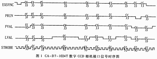
User bus interface signals include: 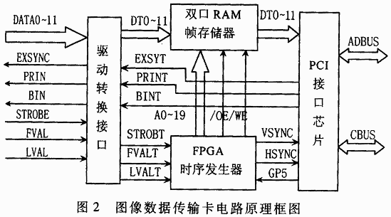
2 Design and implementation of digital CCD camera image data transmission card