Keywords: software radio modulator digital upconverter The basic idea of ​​the software radio SDR (Sofa Radio / Sofa-Defined Radio) developed in the 1990s is to construct an open, standardized, and modular general-purpose hardware platform that implements various functions with software. This is a brand-new idea, and it has received extensive attention once it has been proposed. However, so far, the research on software radio in various countries is still very limited. Because the premise of software radio implementation is highly digital, and the device level at this stage cannot meet the requirements, and the design of software radio lacks a unified standard, so the structure of software radio can only be used to properly adjust its structure according to system requirements. Perform system design. This paper adopts the design method and layered design idea of ​​the combination of programmable devices and special devices, gives a design and implementation method of a general-purpose modulator based on software radio, and gives the test results of the system. 1.1 Block diagram of the overall scheme The general scheme block diagram of the general modulator is shown in Figure 1. There are four main devices used in the system: general-purpose DSP, programmable logic device (FPGA), programmable digital up-converter and D / A converter. Two of the main chips: General DSP and FPGA are general programmable devices. In this way, in the system design, there is the problem of function definition of general devices. In order to make the functions of the system be reasonably distributed among the devices, make full and effective use of chip resources, and make the system design simple and clear, a layered design method is adopted on the basis of the software radio architecture It is divided into three layers: interface layer, configuration layer and processing layer. (1) Interface layer The interface layer is used to communicate with the outside world and control the working mode of the entire system. The interface adopts the host parallel port (HPI) of DSP. The external controller shown in Figure 1 is a PC, that is, the parallel port of the PC is connected to the HPI port of the DSP and communicates, and transfers the control parameters of the system working mode to the DSP. It should be pointed out that any device or instrument with parallel communication mode can replace the PC and control the working mode of the system. The configuration layer is used to configure parameters for the processing layer and is done by the general DSP. DSP calls the corresponding program according to the control parameters received by its host parallel port, calculates the various parameter values ​​required by the configuration layer, and generates corresponding timing signals, and configures the calculation results to the programmable device FPGA and digital upconverter. (3) Processing layer The processing layer is composed of FPGA, digital up-converter and D / A converter. When the parameters of FPGA and digital upconverter are configured, the processing layer works separately from the configuration layer. The FPGA generates I and Q signals corresponding to a specific bit stream and a specific modulation method, and generates a specific timing signal to write the I and Q signals to a digital upconverter to complete the modulation process, and then the D / A converter changes the digital signal Analog modulated signal output. 1.2 The working process of the system The working process of the system is shown in Figure 2. The initial state of the system is that the DSP waits for the host interface (HPI) interrupt. When the DSP receives the host interface interrupt, it calls the interrupt program. This interrupt routine will cause the DSP to perform the following steps: (1) First set the XF pin of the DSP high. This signal becomes low to make the processing layer exit the working state, enter the parameter configuration state, and at the same time give up the bus, and enable the DSP to gain control of the bus; (2) The DSP receives the relevant parameters of the control system working mode from the host parallel port; (3) The parameters required by the DSP calculation processing layer; (4) The DSP writes the parameters to the corresponding address of the processing layer; (5) The DSP sets the XF pin low, gives up control of the bus, and causes the processing layer to take over the bus and enter the working state. (6) The DSP re-enters the state of waiting for host interface interruption. The system can change the working mode and reconfigure the parameters as needed at any time. 2 hardware implementation The hardware structure of the system is relatively simple and is basically the same as the structure of the overall scheme block diagram. The main devices are: TI's DSP chip TMS320VC5402, ALTERA's FPGA chip EPF10K30RCC240, HARRIS's digital upconverter HSP50215 and D / A converter HI5741. 2.1 Interface design This design fully considers the design of the interface between the system and the outside world? Smoke makes the system very open and flexible. The 8-bit parallel host interface of TMS320VC5402 contains many control signal lines, so that it can be directly connected to the 25-pin parallel port through two triggers. External equipment or devices can conveniently control the system's working mode and status through this parallel port. In the internal logic design of EPF10K30, there is a random bit stream generation module. In this module, the input interface of the bit stream signal is also designed, so that the system can modulate the bit stream generated by itself or the externally input bits. Stream modulation. In addition, external interfaces are also designed on the reference clock input pins of EPF10K30 and HSP50215. Through these interfaces, external clock signals can be used to conveniently control the reference clock of the system to meet the needs of users. 2.2 Bus control Bus control includes two aspects: bus level conversion and bus control handover. Because HSP50215 and EPF10K30 are + 5V TTL devices, and the pins of TMS320VC5402 are + 3V TTL levels, level conversion is required. The chips used are level-shifting chips with three-state output, SN74LS16244 and SN74LS16245. The former is a unidirectional chip used for address bus; the latter is a bidirectional chip used for data bus. It can be seen from Figure 1 that some signal lines of the system have multiplexing problems. These signal lines include: HSP50215 data, address bus and write control signal line WR. They are connected to the corresponding signal lines of DSP and FPGA at the same time, so the problem of bus conflicts must be dealt with. Figure 3 shows the bus control circuit design. As can be seen from Figure 3, the XF, HOLDA, and HOLDS signals of the DSP are connected to the bus control module in the EPF10K30 as a handshake signal. Among them, XF is the external flag signal of TMS320VC5402, and it can be set high or low with the command "SSBX XF" or "RSBX XF". When the DSP abandons the bus, set XF low. At this time, FPGA sets the HOLD low, so that the DSP enters the HOLD state. When the HOLDA also goes low, the FPGA takes the bus. When the DSP wants to return to the bus, set XF high. At this time, FPGA immediately abandons the bus, and at the same time sets the HOLD pin high, so that the DSP exits the HOLD state. In addition, the non-signal of the HOLD signal of the DSP is connected to the enable signal of the bus level conversion chip. This can ensure that there is no bus collision problem. The write control signal WR of HSP50215 is also processed similarly. 3 software design The software design of the system includes two parts: FPGA internal logic and control design, and the calculation and configuration of the system parameters. The internal design of FPGA is mainly completed from the generation of baseband bit stream signals to the generation of I and Q signals corresponding to different modulation methods, different information bits, and different code rates. In addition, it also includes bus control logic and chip selection signal generation. The parameters of the system include three parts: the system working mode control parameters transmitted to the HPI port of the DSP, the internal parameters of FPGA, and the parameters of the digital upconverter. The parameter structure of the system can be represented by Figure 4. The operating mode control parameters of the system mainly have the following three: modulation mode, baseband bit stream rate and carrier frequency. These three parameters are passed to the HPI port of the DSP by the external controller through the parallel port. They are at the top layer and are the basic basis for determining the parameters of the lower layer. There are also three internal parameters of FPGA: the ratio of the baseband bit stream rate to the FPGA clock frequency, the number of bits of the serial-to-parallel conversion of the baseband bit stream, and the starting address of the IQ signal in the lookup table. These three parameters are determined by the baseband bit stream rate and modulation method, respectively. The shaping filter parameters also have the following three for root raised cosine or raised cosine filters: rolling coefficient α, interpolation multiple IP, and number of symbol periods crossed DS. These three parameters are intermediate parameters. They are not directly configured in the digital upconverter, but are parameters for calculating the shaping filter coefficients. According to the operating mode control parameters of the system, the optimal shaping filter parameters can be determined. Digital upconverter parameters, that is, HSP50215 internal parameters, the number is relatively large, including: resampling frequency high and low control words; carrier frequency high and low control words; modulation mode control words; gain control words; FIFO depth control words; shaping Filter polynomial control word (including DS and IP); reset control word; synchronous start control word and 256 shaping filter coefficients for each of I and Q. A total of 522 parameters need to be configured. These parameters are determined according to the operating mode parameters and shaping filter parameters of the system. Correctly calculate the above parameters, and correctly configure the chip EPPF10K30 and HSP50215, you can get the correct modulated signal. In this experiment, the real-time spectrum analyzer TEK3086 was used to observe various modulated signals generated by the system. Figure 5 shows some observation results, including BPSK, QPSK, 8PSK, and GSK. The symbol rates of the baseband I and Q signals of various modulated signals in Figure 5 are 5ksps, and the carrier frequency is 1MHz. Each picture contains four small pictures. The upper left corner is the spectrum diagram of the intermediate frequency signal; the upper right corner is the constellation diagram; the lower left corner is the eye diagram of the I channel signal; the lower right corner is the eye diagram of the Q channel signal. The opening of the eye diagram and the degree of dispersion of the various vector points in the constellation diagram (the magnitude of the vector amplitude error) indicate the size of the intersymbol interference and noise in the system, and are also two important parameters to measure the performance of the modulator. Figure 5 (a), (b), (c) uses a root-raised cosine shaping filter, interpolation multiple IP = 16, the number of symbol periods spanned DS = 4, roll-off coefficients are: 0.5, 0. 7 and 0.7. Figure 5 (d) uses a Gaussian shaping filter with IP = 16, DS = 5, and BT = 0.3. Comparing these four graphs, it can be seen that the BPSK and GMSK modulated signals have the largest eye opening, the smallest vector amplitude error, and the best signal performance, followed by the QPSK signal, the 8PSK signal has the smallest eye opening, and the largest vector amplitude error, consistent with theoretical analysis . From the measurement results, the system has better performance and has certain practical value. The experiment proves that the overall scheme of the software-based multi-functional modulator and the internal hardware and software design are correct and feasible. The system has good openness, versatility and scalability, and the obtained modulated signal has good performance. According to the requirements of the working mode of the system, the optimal processing layer parameters are calculated, and the modulated signal with the best performance will be obtained. In addition, if you add a level of amplifying circuit after D / A to increase the transmit power of the signal, the output modulated signal will have better performance. UFO Led High Bay Light,UFO High Bay Led,UFO High Bay Light,Led UFO High Bay Light Jilin Province Wanhe light Co.,Ltd , https://www.wanhelight.com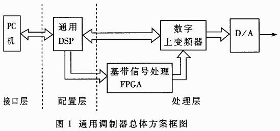
1 Overall design plan 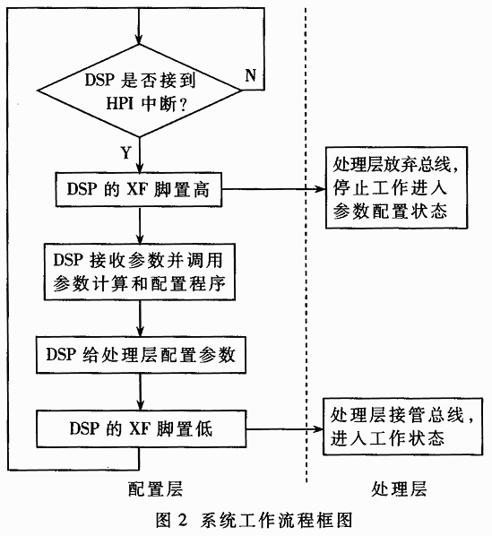
(2) Configuration layer 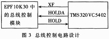

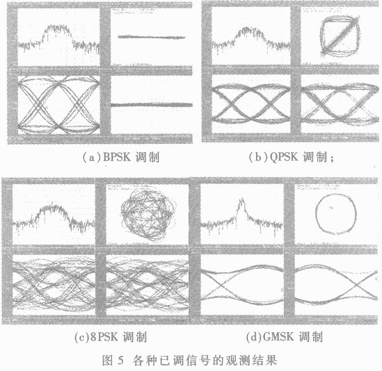
4 Measurement results
Design and implementation of a general-purpose modulator based on software radio
Abstract: Introduce a design method of a general-purpose modulator based on software radio, give an overall design plan, explain the division of system functions between DSP and FPGA and the system's workflow, the hardware implementation method and software design of key parts , Gives the measurement results.