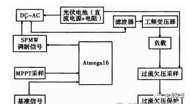
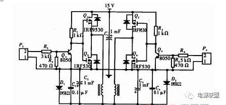
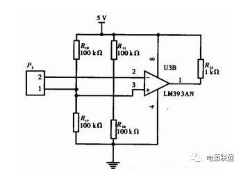
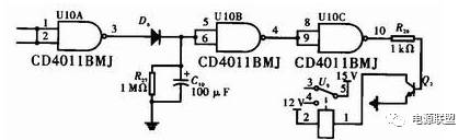
Current sampling circuit design This paper presents an analog grid-connected power generation system that integrates multiple functions such as frequency tracking, maximum power point tracking (MPPT), phase synchronization, input under-voltage protection, output over-current protection, and anti-islanding detection. The system uses the Atmega16 microcontroller for internal timing and control. It leverages the fast PWM function of Timer/Counter T/C2 to generate SPWM signals and utilizes the input capture feature of T/C1 to monitor frequency, phase, distortion, input voltage, and output current. These features enable precise control and efficient operation of the system. The overall system architecture is centered around the Atmega16 microcontroller, which manages the entire control process. A reference sine wave with the same frequency and phase is modulated using SPWM and then amplified through an H-bridge driver. After filtering and transformation via a power frequency transformer, the system outputs a sinusoidal waveform that matches the reference signal in both frequency and phase. Hardware-based protections for overcurrent and under-voltage are implemented, while synchronization, frequency acquisition, and control signal generation are handled by the Atmega16. Figure 1 illustrates the block diagram of the system. Figure 1: System block diagram The hardware design consists of three main parts: the DC/AC drive circuit, the DC/AC converter circuit, and the filter circuit, along with a smoothing capacitor C1. The schematic of the AC/DC converter is shown in Figure 2. Figure 2: AC/DC converter circuit The circuit includes resistors R1–R6, transistors Q3 and Q4, and control terminals P3 and P4. R3 and R4 serve as current-limiting resistors, and their values affect the steepness of the rising edge of the waveform. The RC time constant formed by R1 and R2 with the parasitic capacitance of the collector junction determines the waveform shape. By adjusting R1 and R2, the system can balance between waveform steepness and power consumption. Additionally, the emitter junction’s parasitic capacitance influences the turn-off time of the transistors. To improve switching speed, grounding resistors R5 and R6 are added to accelerate the closing of Q3 and Q4, resulting in a steeper output waveform. In practice, R3 and R5 should be smaller than calculated values to ensure the transistor operates in saturation mode, improving system stability. The DC/AC circuit is composed of two p-channel MOSFETs (Q1, Q2) and two n-channel MOSFETs (Q5, Q6). This configuration simplifies the driving circuit compared to using four n-channel MOSFETs, reducing power loss and heat generation. By controlling the switching speed of the four MOSFETs and passing the signal through a low-pass filter, the DC/AC conversion is achieved efficiently. The filter circuit includes two Schottky diodes 1N5822 as freewheeling diodes to prevent negative voltages. Capacitors C2, C3, C4, and C5, along with inductors L1 and L2, form a low-pass filter. Ceramic capacitors C5 and C6 are used alongside electrolytic capacitors C2 and C3, allowing charge and discharge currents to flow to ground. The inductors L1 and L2 have iron cores, offering better high-frequency performance compared to air-core inductors. The cutoff frequency calculation and component selection are critical for optimal filtering performance. 3 Sampling Circuit 3.1 Current Sampling Circuit Design: Since the load is fixed, current sampling essentially becomes a peak detection process. This circuit functions as a peak detector, where P3 serves as the signal input. Resistors R10, R11, R17, and R18 are adjusted to achieve accurate peak measurement. The resistance values must be fine-tuned based on the signal amplitude. To reduce power consumption and ensure system stability, the resistors are chosen to be as large as possible while maintaining a current more than 10 times the comparator's bias current. The LM393 analog comparator is used, and its output requires a pull-up resistor for proper operation. The circuit is illustrated in Figure 3. Figure 3: Current sampling circuit 3.2 MPPT Sampling Circuit: In photovoltaic systems, it is essential to track the maximum power point (MPP) of the solar cell to maximize energy utilization. The system uses a constant voltage control method for MPPT, which is simple and effective. The core of the circuit is the LM393 comparator, with TL431 providing a reference voltage of 7.5 V. To ensure stability, the current through R3 and R9 must be at least 10 times the comparator's bias current, and these resistors should be as large as possible. Parallel resistors R1 and R2 are used for easier adjustment. An optocoupler U4 isolates the control circuit from the main circuit, preventing interference. The circuit is shown in Figure 4. 3.3 Undervoltage Sampling Circuit Design: The undervoltage sampling circuit uses an analog comparator with a 7.5 V reference voltage at the inverting input. A potentiometer R22 allows for adjustable undervoltage thresholds. The optocoupler U4 provides isolation between the control and main circuits. Resistors R22 and R24 are selected carefully to avoid instability caused by excessive or insufficient current. When the input voltage drops below 7.5 V, the comparator triggers the optocoupler, activating the undervoltage protection circuit to cut off the main power supply. This ensures safe operation under abnormal conditions. 4 Undervoltage and Overcurrent Protection Circuit: The protection circuit, shown in Figure 6, uses a CD4011 quad NAND gate as an inverter, along with a switching diode D6, resistor R27, capacitor C10, transistor 2N3904, and relay. Under normal conditions, the relay remains closed, allowing the system to operate. If an overcurrent or undervoltage condition is detected, the circuit triggers a shutdown, cutting off the power supply. After the fault is cleared, the system automatically resumes operation. The discharge time of R27 and C10 determines the delay before the system restarts, ensuring reliable protection. Figure 6: Undervoltage and overcurrent protection circuit design HA series hood is suitable to small heavy duty connectors, it is widely used in machinery, wind energy, rail transportation, power systems, photovoltaic industry, communications industry, engineering equipment and other fields. Heavy Duty Connector is designed for modular production pre-wiring and satisfying severe environmental conditions, applied in rail transit,industrial automation and equipment manufacturing fields. Compared with traditional wiring methods,use of heavy duty connector can reduce site wiring operation after equipment or vehicle leaves the workshop,enhance production efficiency and reduce quality risk of site wiring. Ha Series Connector,4-Pin Heavy Duty Connector,3 Pin Heavy Duty Connector,Industrial Heavy Duty Kunshan SVL Electric Co.,Ltd , https://www.svlelectric.com