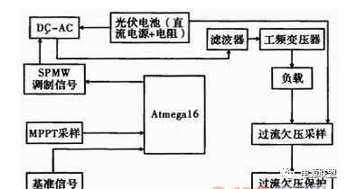
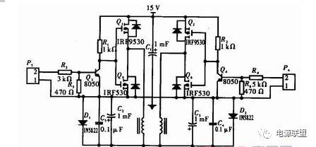
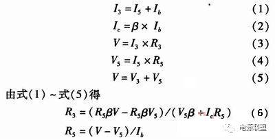
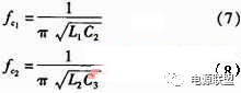
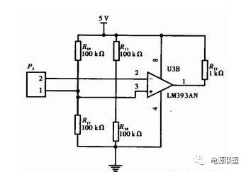
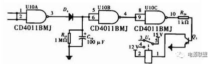
Current sampling circuit design This paper presents an analog grid-connected power generation system that integrates multiple critical functions, including frequency tracking, maximum power point tracking (MPPT), phase synchronization, input under-voltage protection, output over-current protection, and anti-islanding detection. The system utilizes the Atmega16 microcontroller to manage internal timing, PWM signal generation through Timer/Counter T/C2, and frequency and phase monitoring using the input capture function of T/C1. It also detects key parameters such as waveform distortion, input voltage, and output current for control purposes. The overall system design is centered around the Atmega16 microcontroller, which generates a SPWM signal modulated with a reference sine wave of the same frequency and phase. This signal is amplified and used to drive an H-bridge inverter. After filtering and transformation via a power frequency transformer, it produces a sinusoidal current matching the reference signal's frequency and phase. Hardware-based protections, such as overcurrent and under-voltage, are implemented, while synchronization, frequency acquisition, and control signal generation are managed by the Atmega16. The block diagram of the system is shown in Figure 1. Figure 1: System block diagram The hardware design includes three main parts: the DC/AC driver circuit, the DC/AC conversion circuit, and the filter circuit, along with a smoothing capacitor C1. The circuit configuration is illustrated in Figure 2. Figure 2: AC/DC converter circuit The circuit comprises resistors R1-R6, transistors Q3 and Q4, and control terminals P3 and P4. R3 and R4 act as current-limiting resistors, and their values influence the steepness of the waveform's rising edge. A smaller RC time constant results in a steeper rise, but increases power consumption. Therefore, a balance is necessary. Additionally, the emitter junction’s parasitic capacitance affects the turn-off time of Q3 and Q4, so a discharge circuit with R5 and R6 is added to improve switching speed and waveform quality. The base current should be maximized without damaging the transistor, leading to careful resistor selection based on β, Ib, Ic, and other parameters. In practice, R3 and R5 should be smaller than calculated to ensure saturation and system stability. The DC/AC circuit uses two p-channel MOSFETs (Q1, Q2) and two n-channel MOSFETs (Q5, Q6). This configuration simplifies the driving circuit and reduces power loss compared to four n-channel MOSFETs. By controlling the switching speed of these devices and using a low-pass filter, the DC/AC conversion is achieved effectively. The filter circuit consists of two Schottky diodes (1N5822) and capacitors C2-C6, along with inductors L1 and L2. Ceramic capacitors C5 and C6 provide high-frequency filtering, while electrolytic capacitors C2 and C3 handle charge and discharge currents. The inductors have iron cores, offering better inductance at high frequencies. Parameters and cutoff frequency calculations are detailed below. 3 Sampling Circuit 3.1 Current Sampling Circuit Design: Given the fixed load, the current sampling essentially performs peak detection. This circuit is a peak detection circuit with P3 as the signal input. Resistors R10, R11, R17, and R18 are adjusted to achieve peak measurement. The resistance values must be fine-tuned based on the signal amplitude. The current through R14, R15, R19, and R20 must be more than ten times the comparator's bias current, with larger resistances reducing power consumption and ensuring stability. The LM393 analog comparator is used, with its output connected to a pull-up resistor. The circuit is shown in Figure 3. Figure 3: Current sampling circuit 3.2 MPPT Sampling Circuit: In photovoltaic systems, MPPT ensures the solar cell operates at its maximum power point. A constant voltage control method is used here, which is simple and effective. The circuit uses the LM393 comparator and TL431 for a 7.5 V reference voltage. R3 and R9 are chosen to be large, with R1 and R2 in parallel for easy adjustment. The optocoupler U4 isolates the control from the main circuit, preventing interference. The output is controlled by the comparator, triggering SPWM adjustments for constant voltage tracking and MPPT. 3.3 Undervoltage Sampling Circuit Design: The inverting input of the comparator is set to 7.5 V using a potentiometer (R22) for adjustable undervoltage control. The optocoupler U4 provides isolation, and R22 and R24 are sized carefully to avoid instability or damage. When the input voltage drops below 7.5 V, the comparator triggers the optocoupler, activating the undervoltage protection circuit and cutting off the power supply. 4 Undervoltage and Overcurrent Protection Circuit: The circuit uses CD4011 NAND gates, a switching diode D6, resistor R27, capacitor C10, transistor 2N3904, and a relay. When overcurrent or undervoltage occurs, the relay disconnects the power supply. After the fault is cleared, the capacitor discharges through R27, allowing the system to restart automatically. The time interval between faults is determined by T = 2 × R27 × C10. The circuit is shown in Figure 6. Figure 6: Undervoltage and overcurrent protection circuit design M8 distribution box is a kind of industrial connector. It is a device that converts a power supply or data into a shunt and outputs multiple current or data signals. General M8 distribution box refers to the line socket for M8 or M12 specifications of the distribution box. The difference between it and the ordinary socket is that the power output of the ordinary socket is only positive and negative two levels, or there is a ground wire, while the industrial distribution box, the power output is needle I/O port. M8 Distribution Box,D-Sub Input Distribution Box,M8 distribution box 4 way, M8 Junction Box 8 port,M8 distribution box 12 way Kunshan SVL Electric Co.,Ltd , https://www.svlelectric.com