Withstand high voltage up to 750V (IEC/EN standard)
UL 94V-2 or UL 94V-0 flame retardant housing
Anti-falling screws
Optional wire protection
1~12 poles, dividable as requested
Maximum wiring capacity of 6 mm2
high quality Terminal Blocks,6 mm² terminal strips,high performance terminal connectors,BELEKS T06 series connector strips Jiangmen Krealux Electrical Appliances Co.,Ltd. , https://www.krealux-online.com
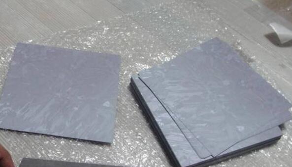
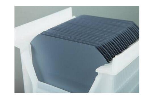
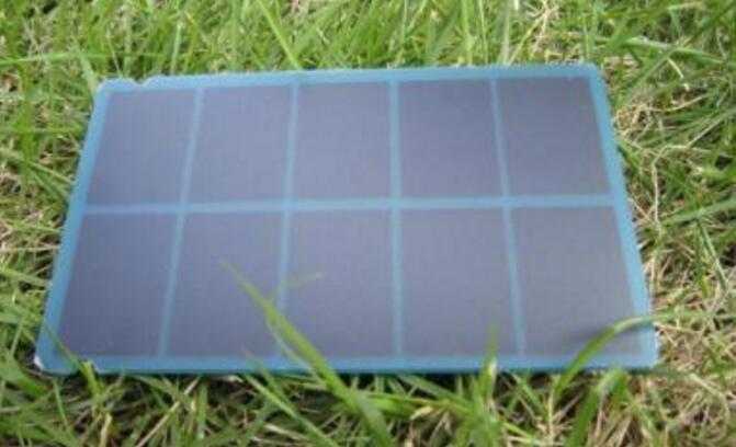
Solar wafer production process analysis _ solar wafers are radiation toxic?
**What is a Solar Wafer?**
A solar wafer is a thin slice of silicon that serves as the base material for photovoltaic cells, which convert sunlight into electricity. These wafers are typically made from crystalline silicon, but other types of solar cells also exist, such as thin-film solar cells, amorphous silicon cells, and concentrated photovoltaic systems.
Solar wafers play a crucial role in renewable energy by transforming sunlight into usable electrical energy. They are widely used due to their high efficiency, energy-saving capabilities, and reliability. Whether installed on rooftops or in large-scale solar farms, they provide a clean and sustainable power source.
**How Do Solar Wafers Work?**
When photons from sunlight hit the surface of a solar wafer, they interact with the semiconductor material—typically silicon—located in a PN junction. This interaction excites electrons, causing them to move and generate an electric current. The voltage produced across the wafer can then be harnessed to power devices or feed into the grid.
One type of solar wafer is the ribbon polycrystalline silicon, which is pulled directly from molten silicon and later cut into square shapes using laser technology. This method reduces mechanical cutting and saves about half the silicon material compared to traditional methods.
**The Production Process of Solar Wafers**
1. **Rounding and Squaring**
The single-crystal silicon rod is cut into a quasi-square shape, and the sharp corners are rounded using a roller mill to prepare it for further processing.
2. **Pickling**
The prepared silicon rod is immersed in an acid solution to remove surface impurities and contaminants, ensuring a clean surface for the next steps.
3. **Adhesive Bonding**
The cleaned silicon bar is bonded to a workpiece plate to secure it during the slicing process.
4. **Slicing**
The bonded silicon rod is mounted on a cutting station, where it is sliced into thin wafers based on specific process parameters.
5. **Cleaning and Degumming**
After slicing, the wafers are pre-cleaned to remove any residual cutting fluid or debris, followed by a degumming process to ensure purity.
6. **Ultrasonic Cleaning**
The wafers are placed in a cassette and cleaned in an ultrasonic bath to remove any remaining particles or contaminants.
7. **Drying**
The cleaned wafers are dried using centrifugal force and heat to eliminate moisture and prepare them for inspection.
8. **Inspection and Packaging**
The final step involves inspecting the wafers for quality, including checking for appearance, thickness, electrical resistivity, TTV (Total Thickness Variation), and warpage. Based on these tests, the wafers are sorted, graded, and packaged for shipment.
**Are Solar Wafers Radioactive or Toxic?**
While the raw materials used in solar wafers, such as silicon, are generally safe, some processes involved in manufacturing can involve chemicals that may be harmful if not handled properly. For example, certain acids used in cleaning or soldering materials may contain lead, which is toxic. However, once the solar wafer is fully manufactured and assembled into a solar panel, it is not considered radioactive or toxic.
That said, the production of solar wafers does involve some environmental concerns, particularly in terms of energy consumption and chemical waste. Nonetheless, the long-term benefits of using solar energy far outweigh these challenges, making solar wafers a key component in the global shift toward clean and sustainable energy.