Fiber Cutter Tool,Fiber Cleaver Kit,Auto Return Cleaver,Single-mode fiber cleaver Guangdong Tumtec Communication Technology Co., Ltd , https://www.gdtumtec.com
Gaoyun Semiconductor Introduces Universal LVDS Transmission Interface Solution
**Foshan, Guangdong, August 22, 2017** – Guangdong Gaoyun Semiconductor Technology Co., Ltd., commonly referred to as "Gaoyun Semiconductor," announced today its support for two key product families: the non-volatile bee® GW1N series and the medium-density Chenxi® GW2A series. These families come equipped with a comprehensive suite of solutions, including a family of LVDS gearbox interface IP cores, complete with soft cores, reference designs, and development boards.
Gaoyun’s GMDS gearbox interface IP is designed to seamlessly switch between clock frequencies and data bit widths between internal logic and external interfaces, ensuring data throughput conservation. This versatile IP not only supports both transmission and reception functions but also offers a variety of transceiver ratios, including 1:1, 1:2, 1:4, 1:7, 1:8, and 1:10. Additionally, the GW1N-6/9 devices support a 1:16 transceiver ratio. The high flexibility of the IP is further enhanced by its ability to accommodate different channel clock and data phase relationships, offering both edge alignment and mid-alignment options.
Gaoyun’s FPGA chips incorporate a dedicated unit module for constructing high-speed LVDS interfaces. These modules work together to meet specific customer demands regarding bandwidth, alignment, transceiver functionality, and transceiver ratios. Key features include:
- **High-speed, low-skew clock HCLK** for high-performance data transmission.
- **GCLK**, the internal system clock, which must be routed via the global clock network.
- A high-speed clock divider module generating a divided clock GCLK synchronized with the input clock HCLK.
- A phase-locked loop module for clock multiplication, division, and phase shifting.
- A serial-to-parallel receiver module for the gearbox function.
- A parallel-to-serial transmitter module for the gearbox function.
- Each I/O pin includes a delay module providing approximately 3200ps of total delay.
Gaoyun’s Universal LVDS gearbox interface IP leverages the embedded dedicated unit modules within the high-cloud FPGA chips, enabling the LVDS I/O interface speed to reach performance levels of 800Mbps to 1.2Gbps. As explained by Gaoyun’s Product Application Manager, Mr. Xu Cai, "In the TCON market application, our FPGA controls the timing actions of the LCD screen, converting input video signals like LVDS into formats suitable for data driving circuits such as Mini-LVDS or RSDS signals, and delivering them to the appropriate data driving circuit at the right time. Our high-cloud FPGA chips align perfectly with the TCON market's demands for LVDS differential pin counts and interface performance."
Mr. Huang Jun, Vice President of Marketing and China Sales Director at Gaoyun Semiconductor, highlighted the rapid advancements in video acquisition and display technologies. "As various high-speed LVDS-based video interfaces like Mini-LVDS, MIPI CSI-2/DSI become increasingly common in mobile phones, tablets, VR, and unmanned systems, there is a growing need for video interface bridging and image processing in user systems." He added, "Gaoyun Semiconductor has developed a universal LVDS gearbox interface solution that combines the strengths of our high-power semiconductor FPGA chips—such as non-volatility, small-thin packaging, and embedded high-capacity SDRAM—to offer consumer and automotive electronics users solutions for video interface bridging and image processing, helping them accelerate their time to market."
---
**Key Features of the IP**
- **Working Frequency**: The LVDS I/O data rate is currently 1.2Gbps; the internal fabric clock rate is 120MHz for the GW1N series and 200MHz for the GW2A series.
**TCON System Architecture and IP Calls**
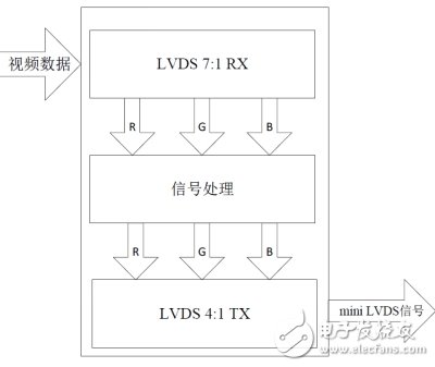
The video image data is first converted into a parallel video signal by the LVDS 7:1 receiving module. Next, the image processing module converts this signal into the format required by the LCD screen. Finally, the mini-LVDS 4:1 transmitting module transmits the processed signal to the LCD screen.
GW1N/1NR and GW2A/2AR series FPGA chips support various differential level standards such as LVDS25, RSDS, LVDS25E, BLVDSE, MLVDSE, LVCECLE, and RSDSE. The I/O logic integrates multiple gear ratios for the switching ratio.
**Development Board and Reference Design**
Gaoyun’s GMDS gearbox interface IP, reference design, and development board support the GW1N-4K FQPF144 package FPGA chip for LVDS receive and mini-LVDS transmit signals. Future upgrades will include support for the GW2A series FPGA chip, enhancing LVDS I/O interface performance.

**About Gaoyun Semiconductor**
Established in January 2014, Guangdong Gaoyun Semiconductor Technology Co., Ltd. is dedicated to developing domestic FPGA solutions and promoting their industrialization. The company aims to launch a national brand FPGA chip with core independent intellectual property rights. Gaoyun Semiconductor strives to provide users with the highest quality service, offering one-stop solutions including chips, design software, soft cores, reference designs, and demonstration boards.
For more information, visit [http://www.gaoyun-semi.com](http://www.gaoyun-semi.com).