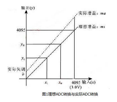
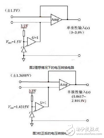
This paper proposes a method for improving the accuracy of the TMS320F2812 ADC, which makes the ADC accuracy effectively improved. The ADC module is a 12-bit, pipelined analog-to-digital converter that controls the data acquisition in the loop. 1 ADC module error definition and impact analysis 1.1 Error definition Commonly used A/D converters mainly exist: offset error, gain error and linearity error. The offset error and gain error are mainly discussed here. Ideally, the ADC module conversion equation is y=x&TImes;mi, where x=input count value=input voltage &TImes;4095/3;y=output count value. In practice, various errors of the A/D conversion module are unavoidable. Here, the conversion equation of the ADC module with gain error and offset error is defined as y=x&TImes;ma±b, where ma is the actual gain and b is Offset error. After multiple measurements of the ADC signal acquisition of the F2812, it is found that the ADC gain error is generally within 5%, which is 0.95. 1.2 Impact Analysis In computer measurement and control systems, the collection of object data generally contains two basic physical quantities: analog and digital. For digital computers, they can be read directly, but the analog quantity can only be accepted by the computer by converting into digital quantities. Therefore, to accurately collect and process the analog quantity, the accuracy and accuracy of analog-to-digital conversion must meet certain requirements. . Because the ADC of the F2812 has a certain offset error of the gain error, it is easy to cause the system to malfunction. The effects of the two errors on the linear voltage input and the A/D conversion result are analyzed below. The ADC module input analog voltage provided by the F2812 user manual is 0 to 3 V. In actual use, the linear input is reduced due to gain error and offset error. The following is an example of y=x&TImes;1.05+80 to calculate the values. When the input is 0, the output is 80. Since the maximum output value of the ADC is 4095, the input maximum voltage value is 2.8013 from the equation y=x×1.05+80. Therefore, the AC input voltage range is 1.4007±1.4007. At this time, the effective number of bits N=ln4015/ln2=11.971, mV/count bit=2.8013/4015=0?6977, and the rest are calculated as above. The last row in Table 1 shows the safety parameters for ADC operation, with the effective number of bits reduced to 11.865 bits and the mV/count bit increased from 0.7326 to 0.7345, which would reduce the conversion result by 0.2%. In practical applications, the acquired signal is often a bipolar signal, so the signal needs to be added to the conversion circuit to convert the bipolar signal into a unipolar signal before being sent to the ADC. A typical conversion circuit is shown in Figure 2. For the ADC module, considering the effect of gain error and offset error on the input range, the conversion circuit needs to be adjusted to the circuit shown in Figure 3. In Figure 3, the reference range of the input gain error has changed. For a bipolar input, the gain error of the 0 V input corresponds to a gain error of 1.4315 V for the unipolar input, so the gain error and offset error of the original ADC are increased. For example, if the ADC has a gain error of 5% and an offset error of 2%, its bipolar gain error is calculated as follows: bipolar input x' = 0.0000 V, unipolar ADC input voltage x = 1.4315 V, The ideal conversion value is ye=1.4315×4095/3=1954, and the actual conversion value is calculated by ya=1954×1.05+80, then the bipolar gain error is ya-ye=2132-1954=178 (9.1%). error). It can be seen from the calculation that the error of the ADC is greatly increased. Therefore, to use the ADC for data acquisition, the ADC must be corrected to improve its conversion accuracy. 2 ADC correction 2.1 correction method It can be seen from the above analysis that the main reason for the poor conversion accuracy of the ADC of the F2812 is the existence of gain error and offset error. Therefore, to improve the conversion accuracy, it is necessary to compensate for the two errors. The ADC module was corrected as follows. Select any two channels of the ADC as the reference input channels, and provide them with their known DC reference voltages as inputs (the two voltages cannot be the same). Obtain the converted value by reading the corresponding result register, using two sets of input and output values. The correction gain and correction offset of the ADC module are obtained, and then the two values ​​are used to compensate the conversion data of the other channels, thereby improving the accuracy of the ADC module conversion. Figure 1 shows how the equation can be used to obtain the correction gain and correction offset of the ADC. The specific calculation process is as follows: 1 Get the converted values ​​yL and yh of the known input reference voltage signal. 2 Calculate the actual gain and offset error using the equation y=x×ma+b and the known reference values ​​(xL,yL) and (xH,yH): Actual gain ma=(yH-yL)/(xH-xL); Offset error b = "yL" - xL x ma. 3 Define the input x=y×CalGain-CalOffset, then the correction gain CalGain=1/ma=(xH-xL)/(yH -yL) from the equation y=x×ma+b, the correction offset CalOffset=b/ma= yL/ma-xL. 4 Apply the corrected gain and correction offset to other measurement channels to correct the ADC conversion result. The above is the whole process of implementing ADC calibration. By using this method, the conversion accuracy of the ADC is greatly improved. Since this method corrects the error of other channels by the error of one channel, it is necessary to ensure a small channel error between the channels by this method. For the F2812ADC conversion module, since the gain and offset error between the channels are within 0.2%, this method can be used to correct it. KNB2-63 Miniature Circuit Breaker
KNB2-63 Mini Circuit breakers, also named as the air switch which have a short for arc extinguishing device. It is a switch role, and also is a automatic protection of low-voltage electrical distribution. Its role is equivalent to the combination of switch. Fuse. Thermal Relay and other electrical components. It mainly used for short circuit and overload protection. Generally, According to the poles, mini Circuit breaker can be divided into 1P , 1P+N , 2P, 3P and 4P.
KNB2-63 Miniature Circuit Breaker,Electronics Miniature Circuits Breaker,Automatic Miniature Circuit Breaker,Mini Circuit Breaker Wenzhou Korlen Electric Appliances Co., Ltd. , https://www.zjthermalrelay.com