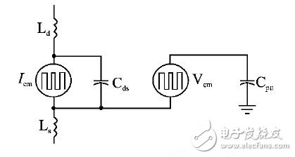
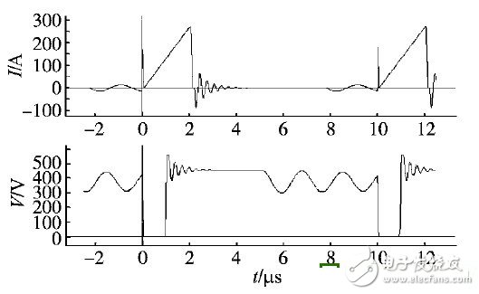
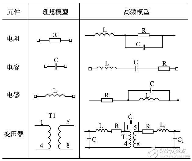
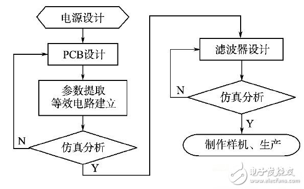
Aiming at the EMC problem that should be considered in the design stage of the switching power supply, the PCB and its structure parasitic parameter extraction and frequency domain simulation methods are introduced. The conduction EMI is predicted during the design stage of the switching power supply, and the influencing factors of the EMI propagation path of the switching power supply are located. On this basis, the basic principles of the switching power supply PCB and its structural design are given. The problems that need to be paid attention to during the EMI prediction process of the switching power supply and the method strategies for reducing the conducted EMI of the switching power supply are analyzed and summarized. 1 Introduction With the increase of switching frequency and the increase of power density, the electromagnetic environment inside the switching power supply is more and more complicated. The electromagnetic compatibility problem has become a major focus in power supply design, and it has become a major difficulty in power supply design work. In the conventional design method, the EMC problem is solved by empirical design, and the EMC problem can be finally considered after the prototype is established. Traditional EMC remedies can only add additional components, and adding components can affect the original control loop bandwidth, resulting in a worst-case redesign of the entire system, increasing design costs. In order to avoid such a situation, it is necessary to consider the EMC problem in the design process, analyze and predict the EMI of the switching power supply, and improve the design according to the mechanism of the interference and its distribution in each frequency band to reduce the EMI level. , thereby reducing design costs. 2 Switching power supply EMI characteristics and classification To predict the conducted electromagnetic interference of the switching power supply, it is first necessary to clarify the mechanism of its generation and the characteristics of the noise source. Due to the high-speed switching action of the power switch tube, the voltage and current change rate are high, the rising edge and the falling edge contain abundant high-order harmonics, so the electromagnetic interference generated is large; the electromagnetic interference of the switching power supply is mainly concentrated on the diode The power switching device and the heat sink and the high frequency transformer connected thereto are connected; since the switching frequency of the switching tube is from several tens of kHz to several MHz, the interference form of the switching power supply is mainly conducted interference and near field interference. Among them, conducted interference will be injected into the grid through the noise propagation path, interfering with other equipment connected to the grid. Switching power conduction interference is divided into 2 categories. 1) Differential mode (DM) interference. The DM noise is mainly caused by di/dt. Through the parasitic inductance, the resistance propagates in the loop between the live line and the neutral line, and the current Idm is generated between the two lines, and does not form a loop with the ground line. 2) Common mode (CM) interference. The CM noise is mainly caused by dv/dt. The stray capacitance through the PCB propagates in the loop between the two power lines and the ground. The interference invades between the line and the ground, and the interference current flows through one-half of each of the two lines. The ground is a common loop; in the actual circuit, due to the unbalanced line impedance, the common mode signal interference will be converted into crosstalk interference that is difficult to eliminate. 3 Simulation Analysis of Switching Power Supply EMI In theory, whether it is time domain simulation or frequency domain simulation, as long as a reasonable analysis model is established, the simulation results can correctly reflect the EMI quantification degree of the system. The time domain simulation method needs to establish a circuit model containing all component parameters in the converter, use PSPICE or Saber software for simulation analysis, and use the fast Fourier analysis tool to obtain the EMI spectrum waveform. This method has been obtained in the analysis of DM noise. Verification. However, nonlinear components such as MOSFETs and IGBTs in switching power supplies have nonlinear characteristics and spurious parameters, which make the model very complicated. At the same time, the circuit topology of the switching power supply circuit changes continuously, resulting in non-convergence in the simulation. problem. When studying CM noise, all parasitic component parameters must be included. Due to parasitic parameters, FFT results are difficult to match with experimental results. Switching power converters usually operate over a large time constant range, including three sets of time constants. : time constant (tens of ms) related to the fundamental frequency of the output; time constant (tens of μs) related to the switching frequency of the switching element; time related to the rise and fall times when the switching element is turned on or off Constant (several ns). For this reason, in time domain simulation, very small calculation steps must be used, and it takes a long time to complete the calculation; in addition, the results obtained by the time domain method often cannot clearly analyze the influence of various variables in the circuit on the interference. The EMI behavior of the switching power supply cannot be deeply explained, and the judgment of the EMI mechanism is lacking, and a clear solution cannot be given for reducing EMI. Frequency domain simulation is an analysis method based on noise source and propagation path impedance model. Use LISN to provide a standard load impedance for noise sources. As seen in Figure 1, the entire system can be reduced to a noise source, a noise path, and a noise receiver (LISN) as seen from the LISN. The frequency domain method can greatly reduce the time of simulation calculation, and generally there is no case where the calculation result does not converge. Figure 1 Noise source and propagation path concept In Figure 1, the noise path includes PCB conduction, coupling path, heat sink capacitive coupling path, transformer coupling path, and so on. 4 SMPS equivalent circuit model based on frequency domain method To perform frequency domain simulation on the switching power supply, first establish a frequency domain simulation model of the switching power supply. Switching power supply EMI frequency domain prediction focuses on the modeling of noise paths, including: high-frequency models of passive components; extraction of PCB and structural parasitic parameters. On the basis of considering the passive components, PCB and structural parasitic parameters, the circuit model of the centralized parameters of the switching power supply is established. The impedance and resonance point of the circuit can be obtained through calculation or simulation, which provides a powerful basis for reducing EMI. Since the propagation paths of differential mode noise and common mode noise are different, it is necessary to separately model the DM propagation path and the CM propagation path. This allows for a better analysis of the characteristics of various disturbances and provides a powerful basis for designing filters. 4.1 Modeling of noise sources Since the DM noise and CM noise need to be analyzed separately, the DM noise source and the CM noise source also need to be separately modeled. M.Nave proposed in the literature [3] that the current source is used as the DM noise source, and the voltage source is used as the CM noise source because the DM noise is mainly caused by di/dt, and the CM noise is mainly caused by dv/dt. Based on this, the literature [4] improved the CM noise source, considering the voltage overshoot and undershoot, and using the DM current source and a voltage source to represent the CM noise source when the line impedance is approximately balanced (eg Figure 2). Figure 2 Representation of common mode noise source The literature basically uses trapezoidal waves to represent the noise source, but in reality, the waveform of the switching device in each circuit can be well approximated by trapezoidal waves. Figure 3 shows a flyback power switch tube. Current and voltage waveforms, in addition to trapezoidal waves, also have current spikes, voltage overshoots, and undershoots, which cause the spectrum of the noise source to be somewhat different from the trapezoidal wave. Therefore, the trapezoidal wave cannot be blindly used to characterize the noise source. Instead, the circuit needs to be analyzed or simulated to obtain the current or voltage waveform of the switching device. Based on this waveform, the noise source is modeled so that the switch can be more accurately reflected. Electromagnetic interference from the power supply. Figure 3 Current and voltage waveform of a flyback power switch 4.2 High frequency model of passive components In the frequency range of EMI, commonly used passive components can no longer be considered ideal, and their parasitic parameters seriously affect their high frequency characteristics. In various passive devices, the high frequency equivalent parasitic parameters of the resistors, inductors, and capacitors can be measured with a high frequency impedance analyzer. Table 1 shows the ideal model and high frequency equivalent model for various passive components. Table 1 High-frequency equivalent model of resistors, capacitors, inductors and transformers For the high-frequency transformer, it is proposed to use the finite element analysis method and the experimental measurement method to obtain the main parameters of the leakage inductance, the primary and secondary self-capacitance and the primary and secondary mutual capacitance, which cause circuit oscillation and increase the conducted EMI. Using Ansoft's Maxwell simulation software, each parasitic parameter can be obtained by finite element analysis by inputting the geometry and electromagnetic parameters of the winding and core of the transformer. The general idea of ​​the experimental measurement method is to derive the equations of the impedance characteristics of the transformer under different working conditions (such as the original secondary winding open circuit and different combinations of short circuits) based on the established model, and then measure the impedance under these conditions, and thus Get leakage inductance and parasitic capacitance. 4.3 Extraction of PCB and structural parasitic parameters In addition to component selection, circuit and its structural design, PCB layout, wiring design, and circuit board processing have a great impact on electromagnetic compatibility, which is a very important design link. Since the PCB layout of the switching power supply is basically manually arranged according to experience, there is great randomness, which increases the difficulty of extracting the PCB distribution parameters. The parasitic parameters of the PCB will cause the impedance change of the noise propagation path of the switching power supply, which affects the control effect of the controller on the output voltage and current of the switching power supply. The unreasonable layout of the PCB will also form a way for the switching power supply to radiate electromagnetic interference, and also absorb external electromagnetic interference through this way, thereby reducing the electromagnetic interference immunity of the switching power supply. Therefore, the layout and layout of the PCB is an extremely important part of the EMC design of the switching power supply. For conducted interference, the extraction accuracy of parasitic parameters is the key to effectively predicting EMI levels through simulation. Although parasitic parameters are easy to calculate for components with simple structures, it is not so easy to obtain parasitic parameters for components in complex structures, such as parasitic parameters of multilayer boards and DC busses. In order to establish a high frequency model of the switching power supply PCB, it is necessary to extract the structural parasitic parameters of the PCB. There are many ways to extract PCB parasitic parameters. The TDR (Time Domain Reflectometry) method can extract parasitic inductance and parasitic capacitance without knowing the actual geometry, but the TDR (Time Domain Reflectometry) method requires a time domain reflectometer. After the prototype is built, this greatly increases the development cost, and the TDR method cannot find the coupling effect in the complex structure; however, the FEA (Finite Element Analysis) method can overcome this shortcoming before the prototype is built. With the FEA tool, the parasitic parameters of the PCB can be accurately obtained, and the coupling of complex geometries can be considered. There are many software for parasitic extraction of PCB structures, such as InCa, SIwave, Q3D, etc., and different methods are used to calculate and extract the parasitic parameters of PCB, such as partial element equivalent circuit method, finite element analysis method, finite element analysis. Method and method of combining moment method. InCa software can only calculate the distributed inductance, is not suitable for calculating the distributed capacitance, and should not deal with the simulation analysis of common mode interference; SIwave software extracts the S parameter of the circuit, which can not clearly reflect the coupling condition in the PCB and its EMI for switching power supply. The influence of Q3D software using FEA and MOM to solve the electromagnetic field can obtain the PEEC partial element equivalent circuit, and can also obtain the mutual inductance of each conductor on the PCB, which can clearly analyze the PCB structure to the switching power supply EMI under various conditions. Impact. J.Ekman proposed a method for establishing an equivalent circuit based on a parasitic parameter matrix, that is, all mutual inductance and mutual capacitance are equivalent to a controlled voltage source, and self-inductance and self-contained connection (equivalent to all mutual inductance and mutual capacitance pairs). The effect of the circuit is equivalent to the controlled voltage source), thus establishing an equivalent circuit model. Figure 4 shows the equivalent circuit model between any two nodes. Figure 4 Equivalent circuit model between any two nodes In Figure 4: Where: Lpmn is the mutual inductance between the two wires of m and n. Although this can improve the accuracy of the simulation, but the calculation amount of the analysis is increased, and the calculation amount can be reduced by ignoring the mutual inductance and mutual capacitance which are not greatly affected by the result. There is a capacitive effect between the heat sink and the switch tube. Noise can propagate between the circuit and the ground through this effect. The influence of the heat sink on the conduction and radiation interference of the switching power supply is described in detail in [9]. There are other noises that are transmitted to the receiver through the inductive or capacitive coupling in space and cannot be ignored. After the model is established, the simulation software can be used to simulate the switching power supply EMI, and the spectrum waveform of the EMI of the switching power supply can be obtained. By analyzing the waveform, the problem of the switching power supply EMI can be located, and the EMI can be reduced by solving the problem. 5 Design methods and strategies for reducing EMI To reduce switching power supply EMI, you need to start with the noise source and propagation path. First of all, for the noise source, the EMI level can be reduced by adding the absorption circuit and reducing the di/dt and dv/dt. However, the efficiency of the switching power supply will be affected, and a certain trade-off between the two needs to be made. . Then there is an improvement to the propagation path. The purpose of the improvement is to increase the impedance of the propagation path to the interference and block its propagation to the receiver. For the power provided by the grid, the impedance is small, thereby increasing the working efficiency of the switching power supply. When selecting components, you need to select components with small influences on parasitic parameters. For example, the ESR and ESL of the capacitor should be as small as possible, and the parasitic capacitance of the inductor should be small. In the design process of the PCB and the position of the heat sink, the impedance to the interference propagation path should also be increased as much as possible so that the noise is transmitted to the receiver through the PCB path as little as possible. If all of the above measures to reduce EMI are completed and the EMC standard has not been met, the filter can be designed based on the differential mode and common mode interference waveforms obtained from the previous simulation analysis. When designing the filter, it is also necessary to pay attention to the layout of the components, as well as the influence of PCB parasitic parameters on the impedance of the filter. The essence is also to increase the impedance to the interference, so that the interference cannot pass through the propagation path. The switching power supply design process is shown in Figure 5. Figure 5 switching power supply design process 6 Conclusion In summary, the current methods for predicting conducted interference of switching power supply are both time domain method and frequency domain method. Since the time domain method requires a small calculation step size, it takes a long calculation time, and the simulation result is not easy. Convergence problem. At the same time, the results obtained by time domain simulation often cannot clearly analyze the influence of various variables in the circuit on the interference. The physical meaning of frequency domain simulation is clear, and it is easier to judge the influence of various parameters on EMI, which can provide a strong basis for reducing EMI. The key issue is to establish a reasonable frequency domain model of interference source and propagation path. There are a lot of software for the extraction of PCB parasitic parameters. These softwares are suitable for different fields and can be selected according to the task requirements. For the high-frequency equivalent circuit model, some methods such as mutual inductance and mutual capacitance that have little influence on EMI can be neglected by the circuit analysis method, which reduces the calculation amount without reducing the excessive calculation accuracy. The main method to reduce EMI is to increase the impedance of the propagation path to electromagnetic interference, so that the electromagnetic interference can pass through the propagation path as little as possible. For the filter design, the simulation results of DM noise and CM noise can be designed separately, and special attention is needed. The component layout of the filter, a good layout can better suppress the propagation of noise. All air springs are sourced globally from manufacturers to the original equipment market with IS9001 and TS16949 and certificates of conformity. All air spring mounting studs and air inlets are covered by protective caps. Where applicable, air springs are supplied complete with the relevant fitting kits. Diaphragm And Airbag,Pneumatic Diaphragm Valve,Diaphragm Control Valve,Diaphragm Solenoid Valve Shenyang Zhicheng Heavy Machinery Manufacturing Co., Ltd. , https://www.zhichengmachinery.com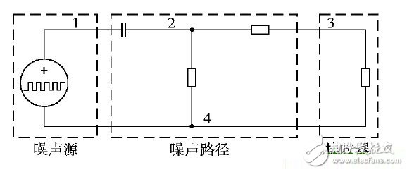

Air springs are produced by a superior manufacturing process which is a reliable steam production method which gives extended service life, durability and constant quality to the rubber diaphragms.