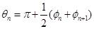
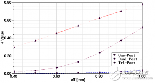
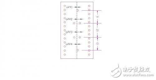
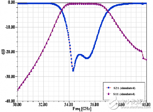
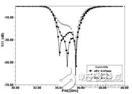
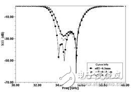
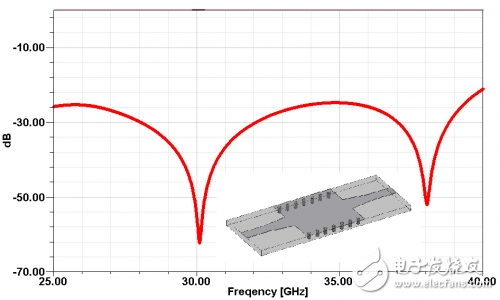
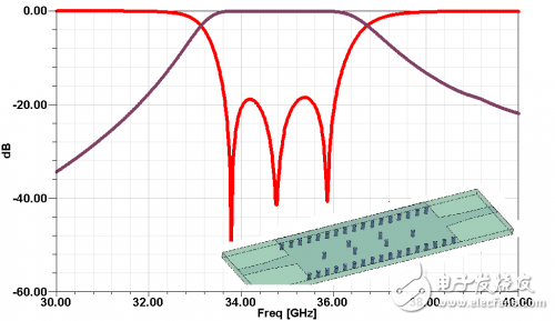
The Ka-band has many interesting features, such as high data transmission rate and good confidentiality, which makes it attract the attention of a large number of engineering and technical personnel. Therefore, a large number of Ka-band commercial and military circuits can be realized. However, the pursuit of low cost, compact structure and high performance will inevitably make the application of new technologies and new concepts inevitable. As one of these new technologies, the increasingly sophisticated LTCC technology has made it possible to implement circuits and components with 3-D structures, including bandpass filters, baluns, transitions and connections, modules and subsystems. Although LTCC technology has broad prospects, it should also pay attention to its own problems, such as electromagnetic isolation between dielectric layers and between different signal paths, heat dissipation of active devices, and processing errors (shrinking and incompatibility of dielectric substrates after co-firing. Avoid media layer offsets, etc.). These factors have seriously affected circuit performance and require special attention from designers. This paper uses LTCC technology to design a relatively stable parallel inductor pin filter. In the design process, one or two shunt inductor pin structures were selected. To further achieve stable performance, the two microstrip-SIW transition structures were compared and the microstrip-SIW transition was finally chosen. Parallel inductor pin filter uses four layers DuPont D943, its relative permittivity er7.4, loss angle The filter initial value is calculated using the following formula: among them The calculated value of the coupling coefficient has the following relationship with the physical structure of the inductor pin: Different numbers of inductive pins correspond to different ranges of variation: When the number of pins is one, the coupling coefficient is the maximum; when it is two, the coupling coefficient is moderate; when it is two, there are almost no coupling between two adjacent resonators, as shown in FIG. 1 . The choice of the number of inductor pins should take into account the calculated value of k. Then calculate the distance (ln) between the adjacent two rows of inductive pins by using equations (7) and (8). The size of the filter is shown in Fig. 2(a), off1=off4=0.1mm, off2=off4=0.35mm, l2=1.75mm, l1=l3=1.58mm; the filter simulation S-parameter is shown in Fig. 2(b). It is worth mentioning that the filter can still maintain good filtering performance when changing off1 (=off4) or off2 (=off3) respectively, as shown in Figure 3 (a), (b). Fig.1 Relationship between eccentricity and coupling coefficient of one to one inductive pin Figure 2 (a) Inductive pin filter parameters Figure 2(b) Inductor Pin Filter Simulation S-parameter Figure 3(a) Changing the insertion loss of an off1 (=off4) filter Figure 3(b) Change the insertion loss of an off2 (=off3) filter Figure 4 Return Loss of Microstrip-SIW Gradient Transition To connect microstrip and SIW, two microstrip-SIW transition structures were proposed. One is the microstrip-SIW gradient transition. Its characteristic is that the structure is simple and the gradient structure can ensure the post-processing performance. However, the quarter-wavelength gradient line also occupies a large area of ​​the substrate. Figure 4; the other is the microstrip-coplanar waveguide-SIW transition, characterized by the use of coplanar waveguide structure to complete the field structure matching, compact structure, but the narrow slotting makes the processing more difficult, it is difficult to guarantee Good experimental results, the simulation results shown in Figure 5. To ensure the performance of the filter, a microstrip-SIW gradient transition structure was chosen. The filter (with transitional structure) simulation S-parameter structure shown in Figure 6: center frequency 35GHz, 1dB relative bandwidth 5.7%, insertion loss within the passband minimum 0.45dB, return loss is better than 21dB. Figure 5 Return Loss of Microstrip-Coplanar Waveguide-SIW Transition Figure 6 Inductor pin filter (and transition structure) S parameters This paper presents a parallel inductor pin filter using LTCC technology. The filter design steps are described. To connect the filter with the microstrip line, the two microstrip to SIW transition structures were compared (Microstrip-SIW Gradient Transition and Microstrip-Coplanar Waveguide-SIW Transition). Filters and transition structures show good simulation results. UV Film,UV Screen Protector,UV Curing Screen Protector Shenzhen Jianjiantong Technology Co., Ltd. , https://www.jjthydrogelprotector.com 0.002, each layer thickness is 0.114mm (after co-fired).
  (1)
(1)  (2)
(2) 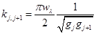 (3)
(3)  (4)
(4)  For the relative bandwidth of the filter, k is the coupling coefficient of the shunt inductor pin structure. In order to simplify the simulation process, a rectangular metal waveguide is used to simulate the SIW. The equivalent width calculation formula is:
 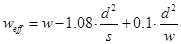 (5)
(5)  (6)
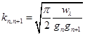
(6)  (7)
(7)  (8)
(8) 
Ka band shunt inductor pin LTCC filter tutorial tutorial
1 Introduction